
Fast%20Timing%20and%20TOF%20in%20HEP PowerPoint PPT Presentation
Title: Fast%20Timing%20and%20TOF%20in%20HEP
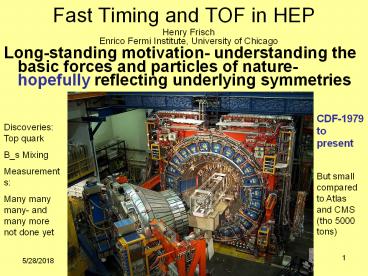
1
Fast Timing and TOF in HEP
Henry Frisch Enrico Fermi Institute, University
of Chicago
- Long-standing motivation- understanding the basic
forces and particles of nature- hopefully
reflecting underlying symmetries
CDF-1979 to present
Discoveries Top quark B_s Mixing Measurements Ma
ny many many- and many more not done yet
But small compared to Atlas and CMS (tho 5000
tons)
2
Fast Timing and TOF in HEP
Henry Frisch Enrico Fermi Institute, University
of Chicago
- 1. Moving from the hadron level to the quark
level- we measure 3-momenta of hadrons, but cant
follow the flavor-flow of quarks. - 2. Quarks are distinguished by different masses-
up and down are light (MeV), strange a few 100
MeV, charm 1.7 GeV, bottom 4.5 GeV, top 170. - To follow the quarks- 2 direct ways- lifetime
(charm,bottom), measuring the mass (strange). - To measure the mass, measure p and v (vL/dt)
3
The unexplained structure of basic building
blocks-e.g. quarks
The up and down quarks are light (few MeV), but
one can trace the others by measuring the mass of
the particles containing them. Different models
of the forces and symmetries predict different
processes that are distinguishable by identifying
the quarks. Hence my own interest.
Q2/3
M2 MeV
M1750 MeV
M175,000 MeV
M300 MeV
M4,500 MeV
Q-1/3
M2 MeV
Nico Berry (nicoberry.com)
4
Fast Timing and TOF in HEP
Henry Frisch Enrico Fermi Institute, University
of Chicago
- I believe that the existence of flavor- up,
down, strange, charm, bottom, and top is
essential, in the sense that if we cant
understand it in a deeper way, were in the grip
of initial conditions rather than fundamental
symmetries or principles. - Disclaimer- View not shared by some (esp. string)
theorists-
5
2 TeV (gt 3ergs) pbar-p collisions
Side View
Beams Eye View
6
A real CDF Top Quark Event
T-Tbar -gt WbW-bbar
W-gtcharm sbar
Measure transit time here (stop)
B-quark
T-quark-gtWbquark
T-quark-gtWbquark
B-quark
Cal. Energy From electron
- Fit t0 (start) from all tracks
W-gtelectronneutrino
Can we follow the color flow through kaons, cham,
bottom? TOF!
7
Application 1- Collider Detector UpgradeCharged
Particle ID
- E.g- Tevatron 3rd-generation detector (combine D0
and CDF hardcore groups) ATLAS Upgrade (true
upgrade)
8
Application 1- Collider Detector Upgrades
- Precision Measurements that rely on measuring
quark-flow
W-mass W-gtcsbar or udbar- different kaon
production Top-mass ttbar -gt WW-bbbar need
to tell b from bbar E.g.- ATLAS, Tevatron-III
9
MW-Mtop Plane
MW 80.398 \pm 0.025 GeV (inc. new CDF
200pb-1) MTop 170.9 \pm 1.8 GeV (March
2007)
10
The Learning Curve at a Hadron Collider (tL)
Application 1- Collider Detector Upgrades
Take a systematics-dominated measurement e.g.
the W mass.
Dec 1994 (12 yrs ago)- Here Be Dragons Slide
remarkable how precise one can do at the Tevatron
(MW,Mtop, Bs mixing, )- but has taken a long
time- like any other precision measurements
requires a learning process of techniques,
details, detector upgrades. Theorists
too(SM)
Electron
Electron-
11
Precision Measurement of the Top Mass
TDR
Aspen Conference Annual Values (Doug Glenzinski
Summary Talk) Jan-05 ?Mt /- 4.3 GeV Jan-06
?Mt /- 2.9 GeV Jan-07 ?Mt /- 2.1 GeV
Note we are doing almost 1/root-L even now
Setting JES with MW puts us significantly ahead
of the projection based on Run I in the Technical
Design Report (TDR). Systematics are measurable
with more data (at some level- but W and Z are
bright standard candles.)
12
Real Possibility
- No SM Higgs is seen at the LHC
- The M-top/M-W plane says the Higgs is light.
- Serious contradiction inside the SM- smoking
gun for something really new - It will be critical to measure M_W and M-top with
different systematics
13
Application 1a- Collider Detector UpgradePhoton
Vertexing
- Atlas Upgrade- Higgs to gamma-gamma?
14
Application 2- Forward LHC Detectors
- - Idea is to do missing-mass search for new heavy
states (e.g. Higgs) by looking at the
quasi-elastic protons forward and backward - Need few psec timing resolution to beat down
backgrounds (accidentals) - Different problems- close to LHC beam (i.e rad
hard), in tunnel, long distances for clock
distribution (but use beam), but few channels-
(small MCPs?) - Good early application- see talks by Christophe,
Krzystof, Andrew,..
15
Application 3-Super-B Factories
- Particle ID for precision b-physics measurements
in larger angle regions - Probe energy frontier via precision/small s
- See talks by Gary and Jerry
16
Application 4 Fixed-target GeometriesParticle
ID and Photon Vertexing
- - Consider LHCb and JPARC KLo-gtp0nn
Geometry is planar- i.e. the event is projected
onto a detection plane. Timing gives the path
length from the point on the plane- Critical new
information for vertexing, reconstruction of p0
s from 2 photons, direction of long-lived
particles. Very thin in z-direction, unlike
Cherenkov counters. Gives a space-point with all
3 coordinates- x,y and z, correlated for
reconstruction- i.e. tomographic. Key new
information- gives tomographic capability to a
plane
17
Application 5- Neutrino Physics
Constantinos Melachrinos (Cypress) (idea of
Howard Nicholson)
- Example- DUSEL detector with 100 coverage and 3D
photon vertex reconstruction.
18
Application 6- Medical Imaging (PET)
19
Characteristics we need
- Feature size lt 300 microns
- Homogeneity (ability to make uniform large-area-
think amorphous semicndtr solar-panel) - Fast rise-time and/or constant signal shape
- Lifetime (rad hard in some cases, but not all)
- System cost ltlt silicon micro-vertex system
20
Detector Development- 3 Prongs
- 1. Electronics- have settled on wave-form
sampling - Already demonstrated by Breton, Delanges,Ritt,
and Varner- many pieces exist, main change is
going to faster process and pooling expertise. - Reasonable precision (see talk by Genat)- few
psec with present rise times, 1 with faster MCP
design. - Gives much more than time- space, pileup, etc.
(Tang) - 2. MCP development- techniques and facilities
(probably) exist- ALD, anodic alumina--will
require industry, natl labs, - 3. Simulation
- Electronics simulation in good shape
- Rudimentary end-to-end MCP device simulation
exists- - Validation with laser teststand and beam line
started
21
GOAL to Develop Large-Area Photo-detectors with
Psec Time and mm SpaceResolution
Too small- can go larger- (But how does
multiplication work- field lines?)
From Argonne MSD ALD web page- can we make cheap
(relatively) ultra-fast planar photo-detector
modules?
22
Generating the signal for relativistic particles
(HEP, nuclear, astro, accelerator)
Incoming rel. particle
- Use Cherenkov light - fast
Custom Anode
Present work is with commercial MCPs e.g.
Burle/Photonis Planicons. Expensive (!), hard to
get, little flexibility. BUT- it works. And well.
23
Design Goals
- Colliders 1 psec resolution, lt 100K/m2
- Neutrino H2O 100 psec resolution, lt 1K/m2
- PET 30 psec resolution, lt 20 of crystal cost
- (but crystal cost not independent of readout!)
Micro-photograph of Burle 25 micron tube- Greg
Sellberg (Fermilab)- 2M/m2- not including
readout
24
Proof of Principle
- Camden Ertley results using ANL laser-test stand
and commercial Burle 25-micron tube - (note- pore size may matter less than current
path!- we can do better with ALD custom designs
(transmission lines))
25
Understanding the contributing factors to 6 psec
resolutions with present Burle/Photonis/Ortec
setups- Jerry Vavras Numbers
- TTS 3.8 psec (from a TTS of 27 psec)
- Cos(theta)_cherenk 3.3 psec
- Pad size 0.75 psec
- Electronics 3.4 psec
26
Photo-multiplier in a Pore
- Idea is to build a PMT structure inside each
pore- have a defined dynode chain of rings of
material with high secondary emissivity so that
the start of the shower has a controlled geometry
(and hence small TTS) - One problem is readout- how do you cover a large
area and preserve the good timing? - Proposed solution- build anode into pores,
capacitively couple into transmission lines to
preserve pulse shape.
27
Psec Large-area Micro-Channel Plate Panel (MCPP)-
LDRD proposal to ANL (with Mike Pellin/MSD)
N.B.- this is a cartoon- working on workable
designs-join us
Front Window and Radiator
Photocathode
Pump Gap
Low Emissivity Material
High Emissivity Material
Normal MCP pore material
Gold Anode
50 Ohm Transmission Line
Rogers PC Card
Capacitive Pickup to Sampling Readout
28
Get position AND timeAnode Design and
Simulation(Fukun Tang)
- Transmission Line- readout both endsgt pos and
time - Cover large areas with much reduced channel
account.
29
Expected PerformanceAnode Design and
Simulation(Fukun Tang)
- Transmission Line- simulation shows 3.5GHz
bandwidth- 100 psec rise (well-matched to MCP) - Board has been made-
30
Scaling Performance to Large AreaAnode
Simulation(Fukun Tang)
- 48-inch Transmission Line- simulation shows 1.1
GHz bandwidth- still better than present
electronics.
31
Front-end Electronics
Critical path item- probably the reason psec
detectors havent been developed
- We had started with very fast BiCMOS designs- IBM
8HP-Tang designed two (really pretty) chips - Realized that they are too power-hungry and too
boutique for large-scale applications - Have been taught by Gary Varner, Stefan Ritt,
Eric DeLanges, and Dominique Breton that theres
a more clever and elegant way- straight CMOS
sampling onto an array of capacitors - Have formed a collaboration to do this- have all
the expert groups involved (formal with Hawaii
and France)- see talks by Tang and Jean-Francois
32
Front-end Electronics
Old plot- apologies (didnt get to update it
before leaving)
33
FY-08 Funds ChicagoAnode Design and
Simulation(Fukun Tang)
34
Jerrys s re-visited Solutions to get to
ltseveral psec resolution.
- TTS 3.8 psec (from a TTS of 27 psec)
- MCP development- reduce TTS- smaller
pores, smaller gaps, filter chromaticity, ANL
atomic-deposition dynodes and anodes. - Cos(theta)_cherenk 3.3 psec
- Same shape- spatial distribution (e.g.
strips and time-differences measure spot) - 3. Pad size 0.75 psec-
Transmission-line readout and shape
reconstruction - 4. Electronics 3.4 psec
fast sampling- should be able to get lt 2
psec (extrapolation of simulation to faster
pulses)
35
Modus Operandi so far
- In Nov. 2005, we had our 1st workshop- idea was
to invite folks working or interested in related
subjects- didnt know many (most) of them - Have developed tools and knowledge- also contact
with pioneers and practictioners (Ohshima,
Howorth, Vavra, Breton, Delanges, Ritt,
Varner) - Development clearly too big for one group-
devices, electronics, applications- have worked
collaboratively with each other, national labs
(see talks by Karen, Andrew,Jerry,), and
industry (Burle/Photonis, Photek, IBM,)
36
My attempt at Goals for the Workshop(these are
my goals- apologies if its presumptious)
- To form collaborations on solving key problems
- To identify expertise- many of these questions
arent new, and somebody (probably Jon or Emil or
Jerry) knows.. - To identify and advertise facilities- e.g. the
Fermilab test beam, ANL laser test-stand, CERN
IBM 0.13micron kit,.. - To answer critical questions along the path(e.g.
2ndary emission of materials,..)
37
My Questions This Time-INote- many questions
from previous workshops have been answered!
- What is the electric field geometry in the MCP
pore? (what are bulk and surface resistivities?
). - What is the response of a nano-carbon film to 200
eV electrons? (photons?) - After the first strike, can the pore be straight?
- If one uses diamond (e.g.), do you really need
fewer strikes?
38
My Questions This Time-IINote- many questions
from previous workshops have been answered!
- Other ways to make pores- e.g. Pierre Jarrons
developments? - Who makes big photocathodes? (Pioneer?)
- Who is interested in learning how to make big
photocathodes for fast timing? - Is there a simulation of the internal workings of
photo-cathodes out there somewhere?
39
My Questions This Time-III
- Can we get a serious simulation effort of the MCP
functions started (collab with Lyon?)? - Funding from NSF Computing, SBIR, a a a a a
European agency? - Are there MCP simulations already out there?
- Can we find a Materials Science group with
students, postdocs, etc. to work with us?
40
Thank you
41
Electronics Simulation-development of
multi-channel CMOS readout
S/N80 ABW 1 GHz Synthesized MCP signal 8 bit
A-to-D
Jean-Francois Genat
42
Simulation and Measurement
- Have started a serious effort on simulation to
optimize detectors and integrated electronics - Use laser test-stands and MTEST beam to develop
and validate understanding of individual
contributions- e.g. Npe, S/N, spectral response,
anode to input characteristics, - Parallel efforts in simulating sampling
electronics (UC, Hawaii) and detectors
(UC,Saclay, Tom Roberts/Muons.inc).
43
Argonne Laser Lab
- Measure Dt between 2 MCPs (i.e root2 times s)
no corr for elect. - Results 408nm
- 7.5ps at 50 photoelectrons
- Results 635nm
- 18.3ps at 50 photoelectrons
44
Work in Progress
- Our way of proceding- use laser test-stand for
development, validation of simulation- then move
to testbeam for comparison with simulation with
beam. - Changes to electronics readout
- Add Ritt and/or Varner sampling readouts
(interleave 10 GS) in works - First test via SMA then integrate chips onto
boards? - Development of 40 GS CMOS sampling in IBM 8RF
(0.13micron)- proposal in draft (ANL, Chicago,
Hawaii, Orsay, Saclay) - Changes to the MCPs
- 10um pore MCPs (two in hand)
- Transmission-line anodes (low inductance-
matched)- in hand - Reduced cathode-MCP_IN MCP_OUT-anode gaps-
ordered - ALD module with integrated anode and capacitive
readout- proposed (ANL-LDRD)
45
Electronics Simulation- Samplinganalog bandwidth
on input at fixed S/N and sampling/ABW ratio
S/N80 Synthesized MCP signal 8 bit A-to-D
Time (fs)
Resolution in femtosec (!)
Jean-Francois Genat
46
Psec Large-area Micro-Channel Plate Panel (MCPP)-
LDRD proposal to ANL (with Mike Pellin/MSD)
Front Window and Radiator
Photocathode
Pump Gap
Low Emissivity Material
High Emissivity Material
Normal MCP pore material
Gold Anode
50 Ohm Transmission Line
Rogers PC Card
Capacitive Pickup to Sampling Readout
47
FY-08 Funds ChicagoAnode Design and
Simulation(Fukun Tang)
48
Electronics Simulation-development of
multi-channel CMOS readout
S/N80 ABW 1 GHz Synthesized MCP signal 8 bit
A-to-D
Jean-Francois Genat
49
Jerrys s re-visited Solutions to get to
ltseveral psec resolution.
- TTS 3.8 psec (from a TTS of 27 psec)
- MCP development- reduce TTS- smaller
pores, smaller gaps, filter chromaticity, ANL
atomic-deposition dynodes and anodes. - Cos(theta)_cherenk 3.3 psec
- Same shape- spatial distribution (e.g.
strips measure it) - 3. Pad size 0.75 psec-
Transmission-line readout and shape
reconstruction - 4. Electronics 3.4 psec
fast sampling- should be able to get lt
1psec (simulation)
50
Muon Cooling position/time station design- LDRD
(ANL) proposal
H.Frisch
Cartoon drawings showing the custom atomic-layer
disposition, the small pores, and the custom
anode configuration (left) and our proposed
module frame (right)
51
Summary
- Next step is to make anodes that give both
position and time- hope is few mm and ltlt 10 psec
resolutions. This would allow systems of (say)
6 by 6 size with 100 channels- good first
step. - Muon cooling is a nice first application of psec
tof- not to big, very important, savings of
money. - We have made a number of false starts and wrong
turns (e.g. the IBM bipolar 200 GHz electronics),
but the fundamentals look good- dont see a hard
limit yet. - Have formed an international community- 2
workshops per year (France and Chicago)- includes
companies (Photonis, Photek, IBM) - Work to be done specifically for muon cooling-
specify a system. Will be easier after testing
next round of anodes. Also needs the sampling
chips.
52
K-Pi Separation over 1.5m
Assumes perfect momentum resolution (time res is
better than momentum res!)
1 Psec
53
Engineering Highlights
- F.Tang (UChicago) designed Voltage Control
Oscillator using IBM 0.13um SiGe BiCMOS8HP - More challenging - Time Stretcher chip (including
ultra low timing jitter/walk discriminator
dual-slope ramping time stretching circuits etc.) - From simulations, accuracy not good enough (5-10
psecs) F.Tang - Power concerns
- NEW Invented 2 new schemes - a) Multi-threshold
comparators, b) 50 GHz 64-channel waveform
sampling. Both schemes give energy and leading
edge time. - Current plan Save waveform and use multiple
thresholds to digitize. Use CMOS (J.F. Genat,
UChicago) - Dec meeting at UChicago with UChicago, ANL,
Saclay, LBL Hawaii, IBM and Photonis
54
MCP Best Results
- Previous Measurements
- Jerry Vavra SLAC (Presented at Chicago Sep 2007)
- Upper Limit on MCP-PMT resolution s MCP-PMT 5
ps - Takayoshi Ohshima of University of Nagoya
(Presented at SLAC Apr 2006) - Reached a s MCP-PMT 6.2ps in test beam
- Using two 10 um MCP hole diameter
- PiLAS red laser diode (635 nm)
- 1cm Quartz radiator (Npe 50)
Burle/Photonis MCP-PMT 85012-501 (64 pixels,
ground all pads except one)
- Use 2 identical 6 micron TOF detectors in beam
(Start Stop) - Beam resolution with qtz. Radiator (Npe 50)
55
RD of MCP-PMT Devices
- We are exploring a psec-resolution TOF system
using micro-channel plates (MCP's) incorporating
- A source of light with sub-psec jitter, in this
case Cherenkov light generated at the MCP face
(i.e. no bounces) Different thicknesses of
Quartz Radiator - Short paths for charge drift and multiplication
Reduced gap - A low-inductance return path for the
high-frequency component of the signal - Optimization of the anode for charge-collection
over small transverse distances - The development of multi-channel psec-resolution
custom readout electronics directly mounted on
the anode assembly ASIC, precision clock
distribution - Smaller pore size Atomic Layer Deposition
56
Atomic Layer Deposition
- ALD is a gas phase chemical process used to
create extremely thin coatings. - Current 10 micron MCPs have pore spacing of
10,000 nm. Our state of the art for Photonis MCPs
is 2 micron (although the square MCPs are 10
micron). - We have measured MCP timing resolution folk-lore
is that it depends strongly on pore size, and
should improve substantially with smaller pores
(betcha).
M.Pellin, MSD
Karen Byrum slide, mostly
57
(No Transcript)
58
(No Transcript)
59
FY-08 Funds ANLLaser Test Stand at Argonne
Hamamatsu PLP-10 Laser (Controller w/a laser
diode head) 405 635nm head. Pulse to pulse
jitter lt 10psec (Manufacture Specs)
Electronics
Lens to focus beam on MCP
Diaphram with shutter to next box
MCP 2
Mirrors to direct light
Mirrors to delay light
50/50 beam splitter
X-Y Stager
Laser Head
MCP 1
Recommended
