
P_3 PowerPoint PPT Presentation
1 / 33
Title: P_3
1
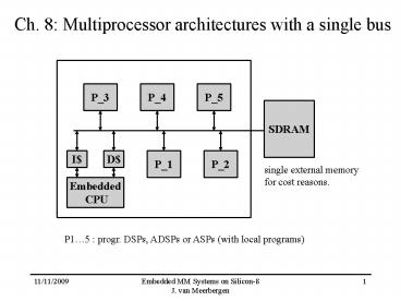
Ch. 8 Multiprocessor architectures with a single
bus
P_3
P_4
P_5
SDRAM
P_1
P_2
I
D
single external memory for cost reasons.
Embedded CPU
P15 progr. DSPs, ADSPs or ASPs (with local
programs)
2
Example TCP chip (TV controller)
- PR3930 peripherals
- Gfx, SDRAM controller,
- Serial interconnect bus,
- I2C, UART, timers
- PI bus architecture
- 80 mm2
- 352 pins
- 0.35 micron process
- 48 MHz (96 for gfx)
D
I
3
Advantages and Disadvantages
- Advantages
- task level parallelism
- efficient solutions
- processors can be optimised for specific tasks
- reuse of IP blocks (Intellectual Property)
- standard bus interfaces (PI bus)
- simple solution (KISS heuristic)
- off-chip memory in an optimized memory process
- Disadvantage
- bandwidth to external memory
- bus memory interface are a central bottleneck
4
Outline
- memories trend towards SDRAM
- internal busses PI bus as an example
- communication protocol
- example H263 application
5
data/bit line BL (column)
Row driver
Row address decoder
Word line (row)
...
Row driver
...
...
...
...
...
...
Row driver
...
Address buffer
Sense Amplifier
Sense Amplifier
Sense Amplifier
...
- precharge BL
- decode row
- discharge BL
- sense amp
- column select
- data gt out
address
Column address decoder and data multiplexer
RAS CAS W/R
Clock generator
Data I/O
6
acces cycle time
RAS
CAS
(a) random access mode
address
row
col
---
---
---
row
Data out
data
Random acces time
7
RAS
CAS
address
c1
c2
c3
c4
c5
c6
c7
---
r
Data out
d1
d2
d3
d4
d5
d6
d7
(c) static column mode
8
Synchronous DRAM (SDRAM)
- introduce a clock (asynchronous gt synchronous)
- pipelining
1 2 3 4 5 6 7 8 9 10 11
12 13 14 15
READ
ACT
READ
PRE
ACT
READ
ROW
COL
ROW
COL
COL
da1
db1
db2
db3
db4
dc1
Hi-Z
CAS latency 1/2/3 for 33/66/99 MHz
Burst length 1/2/4/8/full page
9
Synchronous DRAM (SDRAM)
1 2 3 4 5 6 7 8 9 10 11
12 13 14 15
WRIT
ACT
WRIT
PRE
ACT
WRIT
ROW
COL
ROW
COL
COL
dc3
da1
db1
db2
db3
db4
dc1
dc2
Hi-Z
- Final goal 1 access each clock cycle
- banking
- burst length large enough (e.g. 8)
10
Synchronous DRAM (SDRAM)
1 2 3 4 5 6 7 8 9 10 11
12 13 14 15
READ
ACT
READ
PRE
ACT
READ
ROW
COL
ROW
COL
COL
da1
db1
db2
db3
db4
dc1
db5
db6
db7
db8
CAS latency
11
Synchronous DRAM (SDRAM)
1 2 3 4 5 6 7 8 9 10 11
12 13 14 15
READ
ACT
READ
PRE
ACT
READ
ROW
COL
ROW
COL
COL
dc3
db1
db2
db3
db4
dc1
dc2
da1
db5
db6
db7
db8
12
column
Bank A
Bank B
row
0 --------------7 8------------------15
13
PI Bus (Peripheral Interconnect)
- example of an on-chip bus
- goals low cost (parametrisable),
- medium performance,
- simple protocol
- originally developped within a European OMI
project - further developments PI, Amba (Arm)
14
PI Bus Features
- (single edge) clock synchronous operation
- separate scalable address, data busses
- multiple bus masters
- flexible bus ownership arbitration scheme
default grant mechanism - chaining of bus operations
- wide range of bus operations byte, halfword,
word, 24816 word block - pipelining of bus operations
- peak transfer rate during chained block
transfers 1 data object / clock cycle (e.g. 200
Mbyte/s _at_ 50 MHz, 32 bit) - bus deadlock prevention (timeout)
15
Components (1)
- Bus Master Agent(s)
- A bus agent that initiates communication via
PI-Bus. It issues bus operations once bus
ownership has been granted. - Bus Slave Agent(s)
- A bus agent that responds to bus operations on
PI-Bus when it is selected as target of a bus
operation - Bus Cache Agent(s)
- optional
- A bus agent including a cache memory that keeps
track of PI-Bus communication between a bus
master and a bus slave. It takes appropriate
measures to ensure consistency of its local cache
contents with memory addressed by the bus
operation.
The same block can be master, slave and
cache. Minimum configuration 1 slave and 1 master
16
Components (2)
- Bus Control Unit
- Bus control components that are required for
PI-Bus functionality - arbitration and assignment of bus ownership to
bus masters (system specific! ) - selection of bus slaves (system specific! )
- generation of bus error on an address that is
not mapped to a bus slave - generation of timeout on dead lock
- initiation of memory coherency protocol (system
specific! )
17
Components in a PI-Bus System
Master
Master Slave
Cache
Cache Master Slave
BUS Control Unit
Unlimited number of bus masters bus
slaves bus caches
Slave
Slave
BCU is system specific
Master, slave and cache functionality can be
combined
18
Bus Master
Bus Slave
Dm0
ACK20
OPC40, READ, An,2, LOCK
TOUT
CLK
CLK
REQx
SELy
Bus Control Unit
RESETN
RESETN
GNTx
CLK
RESETN
19
1. Phase 1 REQx gt BCU GNTx
gt master 2. Phase 2 SELy gt slave
master sends An2 and OPC40 and READ
20
3. phase 3 data transfer
slave sends ACK20
21
1 2 3 4
5 6
CLK
driven
Undriven, previous logic state weakly held
OPC, LOCK, A, READ
SEL
Dread
ACK, Dwrite
ACKWAT
ACKRDY
Address cycle
data cycle
data cycle
Bus Operation
22
1 2 3 4
5 6
CLK
Op1 LOCK1
Op2 LOCK0
OPC, LOCK, A, READ
0
SEL
ACK, D
ACKWAT
ACKRDY
ACKRDY
Address cycle
Address/ data cycle
data cycle
Address/ data cycle
2 Bus Operations
23
Complexity slave 0.5 Kgates 0.05 sq. mm.
master 2Kgates 0.2 sq. mm
0.35 micron
Clock speed limited by coupling capacitance
and increased resistance
24
PI-Bus Hierarchy
Processors Memory (Interfaces)
Peripherals System Functions
BUS Control Unit
BUS Control Unit
Bridge
25
PI bus interrupt architecture
interrupt controller
Interrupt sources (IS)
request_1
IC
processor
acknowledge_1
request_2
interrupt request
acknowledge_2
request_3
IS_1
IS_2
IS_3
acknowledge_3
read int_vector
PI-bus
26
interrupt controller
Interrupt sources (IS)
IC
processor
request chain
interrupt request
acknowledge chain
IS_1
IS_2
IS_3
read int_vector
PI-bus
Difference between on-chip and off-chip busses
27
Communication protocol
Processors communicate via SDRAM under control of
the CPU
- from CPU to processor memory mapped
communication - from processor to CPU interrupt
28
Communication protocol discussion
- Advantage simple solution
- Disadvantage
- CPU overloaded with synchronisation
requests (must be kept smaller than 1Khz
typically) - consequence grainsize of tasks must be
sufficiently large ( line 16kHz, stripe
2kHz, frame 50Hz) - halves the bandwidth
- mapping problems central resource limits
scalability, specially with real-time constraints - Alternative polling instead of interrupt
(active wait) - Disadvantage keeps CPU busy
29
225 MHz bus TM core 64 KB I Cache line size
64 B Latency 70 cycles ISR trashes 10 of the
I pSOS send taskswitch receive 6000
cycles Assume 20 video tasks and frame rate 60
Hz ? How much CPU time (in ) is used for
synchronisation
Latency for 1 task switch pSOS send taskswitch
receive 6000 cycles cache trashing assume
10 of 6.4 KB 100 cache lines 70 cycles
7000 cycles som 13 000 cycles 58 us Assume
20 video tasks and frame rate 60 Hz 1200
switches per sec 69 msec 0.069 7 of
cpu-load
30
Example H.263 video encoder
out
VLC
in
IDCT
IQ
Q
DCT
-
Frame store
Motion est.
Pred
SQCIF 96128 px 10 Hz 100 mW
31
PR3940
I
D
memory
10 Hz gt 140 MHz CPU
32
Encode (predict, DCT,Q)
Decode (IQ, IDCT recon)
SAD
SDRAM
Video in
Video out
I
D
Embedded CPU
33
20 Mips 80 mW
Recommended
