
Wafer And Integrated Circuits Report PowerPoint PPT Presentations
All Time
Recommended

United States Wafer And Integrated Circuits IC market competition by top manufacturers/players, with Wafer And Integrated Circuits IC sales volume, price, revenue Million USD and market share for each manufacturer/player; the top players including Entegris, Inc. RTP Company 3M Company ITW ECPS Dalau Brooks Automation, Inc.
| PowerPoint PPT presentation | free to download

Download Free Research Report PDF : http://bit.ly/2MHjlHc A Semiconductor glass wafer is usually a very thin disc used as a base for manufacturing integrated circuits. It is a thin piece of semiconductor material, usually made of borosilicate glass, quartz, or fused silica.
| PowerPoint PPT presentation | free to download

Wafer backgrinding is a semiconductor device fabrication step during which wafer thickness is reduced to allow stacking and high-density packaging of integrated circuits (IC). In the context of China-US trade war and global economic volatility and uncertainty, it will have a big influence on this market. Wafer Backgrinding Tape Report by Material, Application, and Geography ? Global Forecast to 2023 is a professional and comprehensive research report on the world?s major regional market conditions, focusing on the main regions (North America, Europe and Asia-Pacific) and the main countries (United States, Germany, United Kingdom, Japan, South Korea and China).
| PowerPoint PPT presentation | free to download

... stategy meetings, presentations, quizzes. CS252/Patterson. Lec 2.8 ... funny times, as most systems can't access all of 2nd level cache without TLB misses! ...
| PowerPoint PPT presentation | free to view

Wafer-level packaging (WLP) is the technology of packaging an integrated circuit while still part of the wafer, in contrast to the more conventional method of slicing the wafer into individual circuits (dice) and then packaging them. Wafer-Level Packaging includes Fan-in WLP and Fan-out WLP on the base of classification.
| PowerPoint PPT presentation | free to download

A glass wafer is usually a very thin disc used as a base for manufacturing integrated circuits. It is a thin piece of semiconductor material, usually made of borosilicate glass, quartz, or fused silica.In terms of geographic regions, APAC will contribute to major semiconductor glass wafer market growth. This is due to the strong presence of electronics manufacturers. Moreover, the presence of several foundries in countries such as China, Japan, South Korea, and Taiwan will also significantly contribute to the growth of the market in APAC.
| PowerPoint PPT presentation | free to download

Semiconductor Wafer, By Process (BEOL, FEOL), by Application (Consumer Electronics, IT, Healthcare, BFSI, Telecom, Automotive)- Forecast 2016-2022
| PowerPoint PPT presentation | free to download

Global Wafer Fabrication Equipment Market: Size, Trends & Forecasts (2016-2020) research of 65 pages with 28 Figures and 4 Tables, 4 company profiles to the Semiconductor and Electronics industry segment of its online data and intelligence library, now available at http://www.marketreportsonline.com/contacts/purchase.php?name=567546.
| PowerPoint PPT presentation | free to download

Application Specific Integrated Circuit Market Research Report: By Product Type (Full Custom Design, Semi-Custom Design, Programmable) And By Application (It & Telecommunication, Industrial, Automotive, Consumer Electronics) – Global Forecast Till 2023
| PowerPoint PPT presentation | free to download

Global Silicon Wafer Reclaim Market Research Report: By Wafer Diameter (150 MM, 200 MM, 300 MM and others), by Application (Integrated Circuits, Solar Cells, Photoelectric Cells and others), by Region (North America, Europe, Asia-Pacific and Rest of the World) - Forecast till 2025. Silicon wafer reclaim is a multi-step process that transforms a used wafer with multiple layers of various materials into a qualification wafer. The major steps included in wafer reclaim are sorting. stripping, lapping and grinding, polishing, cleaning, and inspection. Browse Complete Report Details: https://www.marketresearchfuture.com/reports/silicon-wafer-reclaim-market-8246
| PowerPoint PPT presentation | free to download
Thin wafer, which are the thin slices of semiconductor, are largely being used for manufacturing integrated circuits (ICs). They are extensively used across automotive sector owing to the elevating demand for AI-chipsets that are developed using thin wafer technology. Get sample copy of this research report @ https://www.gminsights.com/request-sample/detail/5007
| PowerPoint PPT presentation | free to download

Wafer level packaging (WLP) is a method of attaching packaging components to an integrated circuit (IC) prior to dicing the wafer. This procedure varies from a traditional method, which involve slicing the wafer into separate circuits (dice) before attaching the packaging components.
| PowerPoint PPT presentation | free to download

Wafer market by Size (150 mm, 200mm, 300mm, and 450mm), by Type (N-type and P-type), by Application (Solar cells, Integrated Circuits, Photoelectric Cells, and Others) - Forecast 2016-2022
| PowerPoint PPT presentation | free to download
Silicon Wafers industry by Size (150 mm, 200mm, 300mm, and 450mm), by Type (N-type and P-type), by Application (Solar cells, Integrated Circuits, Photoelectric Cells, and Others) - Forecast 2016-2022
| PowerPoint PPT presentation | free to download

Epitaxial wafers are a key component in the semiconductor industry. They are used to produce high-quality, single-crystal layers of semiconductor materials on a substrate, which are then used in the manufacturing of various electronic devices. These wafers are essential for the production of advanced semiconductors, such as integrated circuits, power devices, and sensors. The demand for epitaxial wafers is driven by the growing need for advanced and efficient electronic devices across various industries.
| PowerPoint PPT presentation | free to download

Wafer reclaim is a silicon wafer which has been polished, cleaned and processed so that they can be used for the different applications such as solar cells, integrated circuits and others. The costs of this reclaimed wafer are very less and the quality is very good as well. These silicon wafers are thin in size and caters same features as the virgin test wafers. They are mainly used in integrated circuits and many companies also use these silicon wafers for their product testing.
| PowerPoint PPT presentation | free to download

With the rapid expansion in the electronics industry, there has been increasing demand for microelectromechanical systems (MEMS), microchips and integrated circuits for manufacturing various consumer electronic goods, including smartphones, laptops and desktops Get a PDF Sample for more detailed market insights: Visit the following link: https://www.imarcgroup.com/semiconductor-wafer-polishing-grinding-equipment-market E-mail: sales@imarcgroup.com Contact: +91-120-415-5099
| PowerPoint PPT presentation | free to download

Gallium Arsenide (GaAs) Market Size is forecast to reach $2.2 billion by 2027, growing at a CAGR of 11.1% during 2022-2027. GaAs is increasingly used as a replacement for silicon because of its enhanced electronic properties and was selectively grown on GaAs substrates patterned with SiO2 by conventional molecular beam semiconductor device epitaxy. Moreover growing demand for GaAs solutions such as laser diodes, light emitting diodes, optoelectronic devices and Monolithic Microwave Integrated Circuits across various end-user industries such as aerospace & defense, electronics, and communications is analyzed to drive the GaAs Wafer Market share.
| PowerPoint PPT presentation | free to download

In microelectronics, a three-dimensional integrated circuit (3D IC) is an integrated circuit (IC) manufactured by stacking silicon wafers or dies and interconnecting them vertically using, for instance, through-silicon vias (TSVs) or Cu-Cu connections. In the context of China-US trade war and global economic volatility and uncertainty, it will have a big influence on this market. 3D Semiconductor Packaging Report by Material, Application, and Geography ? Global Forecast to 2023 is a professional and comprehensive research report on the world?s major regional market conditions, focusing on the main regions (North America, Europe and Asia-Pacific) and the main countries (United States, Germany, United Kingdom, Japan, South Korea and China)
| PowerPoint PPT presentation | free to download

Lithography equipment is widely used and designed for printing complex circuit designs on silicon wafers which are mostly raw materials for integrated circuits (ICs).
| PowerPoint PPT presentation | free to download

Advanced packaging is specially designed to improve the device performance by using integrated circuits which protect the metallic part from damaging. 3D integrated circuits, 2.5D integrated circuits, fan out wafer level package and among others are some of the common types of advanced packaging technologies. Different types of integrated circuits are manufactured as per the need of the packaging. They are widely used in industries such as healthcare, automotive, aerospace, defense and others.
| PowerPoint PPT presentation | free to download

Wafer Cleaning equipment market report categorizes the global market based on types, equipment, and applications forecasting revenue of wafer cleaning equipment market from 2012 to 2017.
| PowerPoint PPT presentation | free to download

According to the latest research report by IMARC Group, The global wafer level packaging market size reached US$ 4.8 Billion in 2022. Looking forward, IMARC Group expects the market to reach US$ 13.2 Billion by 2028, exhibiting a growth rate (CAGR) of 18.3% during 2023-2028. More Info:- https://www.imarcgroup.com/wafer-level-packaging-market
| PowerPoint PPT presentation | free to download

Market Research Future published a research report on “Silicon Wafers Market Research Report- Global Forecast 2022” – Market Analysis, Scope, Stake, Progress, Trends and Forecast to 2022. Get complete Report @ https://www.marketresearchfuture.com/reports/silicon-wafers-market-2052
| PowerPoint PPT presentation | free to download

According to the latest research report by IMARC Group, The global e-beam wafer inspection system market size reached US$ 631.3 Million in 2022. Looking forward, IMARC Group expects the market to reach US$ 1,921.1 Million by 2028, exhibiting a growth rate (CAGR) of 21.44% during 2023-2028. More Info:- https://www.imarcgroup.com/e-beam-wafer-inspection-system-market
| PowerPoint PPT presentation | free to download

Application Specific Integrated Circuit Market Research Report: By Product Type (Full Custom Design, Semi-Custom Design, Programmable) And By Application (It & Telecommunication, Industrial, Automotive, Consumer Electronics) – Global Forecast Till 2023
| PowerPoint PPT presentation | free to download

Silicon wafer reclaim is a type of multi-step procedure which transforms a used wafer with numerous layers of various materials into a qualification wafer. The major steps integrated in wafer reclaim are sorting, stripping, lapping and grinding, polishing, cleaning and the inspection.
| PowerPoint PPT presentation | free to download
TRD Status Report
| PowerPoint PPT presentation | free to download

Indium Phosphide Wafer Market Size is forecast to reach $82.8 million by 2026, at a CAGR of 8.12% during 2021-2026. The indium phosphide wafers offers a superior electron velocity as compared to other popular semiconductors such as silicon.
| PowerPoint PPT presentation | free to download

Silicon on insulator is a fabrication technique that mainly uses pure form of crystal silicon and silicon oxide for microchips and integrated circuits. This technology also uses layered silicon–insulator–silicon substrate in place of conventional silicon substrates which are applicable for manufacturing of semiconductors. This technology is having many applications in SOI wafers, high performance radio frequency, microelectronics and photonics.
| PowerPoint PPT presentation | free to download

Indium Phosphide Wafer Market Size is forecast to reach $82.8 million by 2026, at a CAGR of 8.12% during 2021-2026.
| PowerPoint PPT presentation | free to download

Indium Phosphide Wafer Market Size is forecast to reach $82.8 million by 2026, at a CAGR of 8.12% during 2021-2026.
| PowerPoint PPT presentation | free to download

Global 3D Integrated Circuit Market, by Application (Medical, Automotive, Consumer electronics, Military), by Component (Sensors, Diodes, MEMS, Interposer), by 3D Technology (Wafer-level packaging, System Integration) -2022
| PowerPoint PPT presentation | free to download

Global Silicon Wafers Market is expected to reach USD 11,889.0 Million by 2025 at a CAGR of 3.19% during the forecast period. Market Research Future (MRFR), in its report, envelops segmentation and drivers to provide a better glimpse of the market in the coming years. Get Complete Report @ https://www.marketresearchfuture.com/reports/silicon-wafers-market-2052
| PowerPoint PPT presentation | free to download

Semiconductor Silicon Wafer Market By Process (BEOL, FEOL), by Application (Consumer Electronics, IT, Healthcare, BFSI, Telecom, Automotive) - Forecast 2022
| PowerPoint PPT presentation | free to download

semiconductor wafer market share By Process (BEOL, FEOL), by Application (Consumer Electronics, IT, Healthcare, BFSI, Telecom, Automotive)- Forecast 2016-2022
| PowerPoint PPT presentation | free to download

semiconductor wafer fabrication market By Process (BEOL, FEOL), by Application (Consumer Electronics, IT, Healthcare, BFSI, Telecom, Automotive)- Forecast 2016-2022
| PowerPoint PPT presentation | free to download
semiconductor wafer market size By Process (BEOL, FEOL), by Application (Consumer Electronics, IT, Healthcare, BFSI, Telecom, Automotive)- Forecast 2016-2022
| PowerPoint PPT presentation | free to download
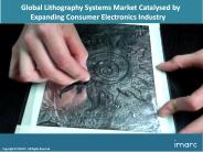
Get more information about the market: https://www.imarcgroup.com/lithography-systems-market According to the latest report by IMARC Group, titled “Lithography Systems Market: Global Industry Trends, Share, Size, Growth, Opportunity and Forecast 2018-2023”, the global lithography systems market reached a value of more than US$ 8.1 Billion in 2017. Lithography, also known as photolithography or semiconductor lithography, is the process of creating the patterns, shapes, locations and dimensions of numerous components in an integrated circuit (IC). These patterns are drawn on silicon wafers using a light sensitive polymer called photoresist. Want more information about this market? Request a free report sample: https://www.imarcgroup.com/request?type=report&id=904&flag=B Contact Us IMARC Group USA: +1-631-791-1145 Email: sales@imarcgroup.com Website: https://www.imarcgroup.com Follow us on twitter : @imarcglobal
| PowerPoint PPT presentation | free to download

The glass wafer market was valued at US$ 295.48 million in 2020 and is projected to reach US$ 575.17 million by 2028; it is expected to grow at a CAGR of 8.5% from 2020 to 2028.
| PowerPoint PPT presentation | free to download

ICT development report of China Embassy of the People s Republic of China in the Republic of India Contents The basic conditions and trends of China's ICT An ...
| PowerPoint PPT presentation | free to download

Global silicon wafer reclaim market is set to witness a steady CAGR of 4.15% in the forecast period of 2019- 2026. The report contains data of the base year 2018 and historic year 2017. Rising demand for consumer electronic goods and increasing demand of product from solar energy industry are the factor for the growth of this market.
| PowerPoint PPT presentation | free to download
Gallium Arsenide (GaAS), a mixture of gallium and arsenic, is a compound semiconductor of Gallium that is formed by melting of metals such as aluminum and zinc and Arsenic. While gallium is said to be rarer than gold, arsenic is known to be poisonous.
| PowerPoint PPT presentation | free to download
ICT development report of China The Ministry of Science and Technology of the People s Republic of China Contents The basic conditions and trends of China's ICT An ...
| PowerPoint PPT presentation | free to download
Paul Dauncey, Imperial College London. Representing the CALICE Collaboration. 30 October 2002. Paul Dauncey - CALICE/PRC ... FANAL. Photons multiplicity/event ...
| PowerPoint PPT presentation | free to download

This report studies the global Electronic Grade Phosphoric Acid market status and forecast, categorizes the global Electronic Grade Phosphoric Acid market size (value & volume) by manufacturers, type, application, and region. This report focuses on the top manufacturers in North America, Europe, Japan, China, India, Southeast Asia and other regions (Central & South America, and Middle East & Africa).
| PowerPoint PPT presentation | free to download

Silicon wafer reclaim market size is valued at USD 2,353.94 million by 2028 is expected to grow at a compound annual growth rate of 17.05% in the forecast period of 2021 to 2028
| PowerPoint PPT presentation | free to download

Bharat Book Bureau provides the report, on “The Global Market Report on Electronic chemicals and Materials ” The Report Provide basic View on Electronic chemicals and materials are solid, liquid and gaseous substances used in the fabrication of semiconductors and printed circuit boards (PCBs).
| PowerPoint PPT presentation | free to download

Indium Phosphide Wafer Market Size is forecast to reach $82.8 million by 2026, at a CAGR of 8.12% during 2021-2026.
| PowerPoint PPT presentation | free to download

Indium Phosphide Wafer Market Size is forecast to reach $82.8 million by 2026, at a CAGR of 8.12% during 2021-2026.
| PowerPoint PPT presentation | free to download

Bharat Book Bureau provides the report on “Global Electronic Chemicals Market Forecast, 2012 - 2026”, (https://www.bharatbook.com/materials-chemicals-market-research-reports-751124/global-electronic-chemicals-semiconductor-ic-pcb.html)The report provides increasing demand for miniaturization of electronic components, anticipated to aid global electronic chemicals market in the coming years.
| PowerPoint PPT presentation | free to download

Global indium phosphide compound semiconductor market size is expected to reach $9.7 Bn by 2028 at a rate of 11.2%, segmented as by product, power semiconductors, transistors, integrated circuits, diodes and rectifiers, other products
| PowerPoint PPT presentation | free to download

Looking forward, the e-beam wafer inspection system market value is projected to reach a strong growth during the forecast period (2021-2026). More info:- https://www.imarcgroup.com/e-beam-wafer-inspection-system-market
| PowerPoint PPT presentation | free to download

Review of Engineer 2020 Phase I Report Phase I: Creating the Vision Phase I: Visions and scenarios of engineering practice Phase II: Action agenda to shape the future ...
| PowerPoint PPT presentation | free to view

Indirect optical control of microwave circuits and antennas Amit S. Nagra ECE Dept. University of California Santa Barbara Acknowledgements Motivation for Optical ...
| PowerPoint PPT presentation | free to download