
Bipolar Junction Transistors PowerPoint PPT Presentations
All Time
Recommended

To take both injection efficiency and base transport factor into account alpha ... To make the base width independent of the collector voltage the base ...
| PowerPoint PPT presentation | free to view
The narrated power point presentation attempts to explain the transistor working principles, different transistor configurations and characteristics at different transistor configurations.
| PowerPoint PPT presentation | free to download

Bipolar Junction Transistors (BJTs) Types of BJTs NPN PNP NPN-BJT Structure n-type p-type n-type NPN BJT Symbol E B C PNP-BJT Structure p-type n-type p-type PNP BJT ...
| PowerPoint PPT presentation | free to view

Bipolar Junction Transistors ... Ensure Transistor CKT will work over the range of specified voltage, tempertature, and transistor variation.
| PowerPoint PPT presentation | free to view

Except for reversal of current directions and voltage polarities, the pnp BJT is almost identical to the npn BJT. Title: No Slide Title Author: U95-2 Last modified by:
| PowerPoint PPT presentation | free to view

This article discuss about the Bipolar Transistor also called Bipolar Junction Transistors or BJT including the Types, working and applications
| PowerPoint PPT presentation | free to download

The physics of
| PowerPoint PPT presentation | free to view

Lecture 27 Bipolar Junction Transistors Bipolar Junction Transistors Tubes Deforest s Audion Triode Tube Bardeen, Brittain and Shockley First Transistor Initial ...
| PowerPoint PPT presentation | free to view

Biasing the BJT. Bias Stability. Small Signal Models. Single Transistor Amplifiers ... DC Bias. C. Hutchens Chap 4 ECEN 3313 Handouts. 18. Self Biased with RE ...
| PowerPoint PPT presentation | free to view

Chapter 02 Bipolar Junction Transistors (BJT s) 2.1 Device Structure and Physical Operation 2.2 Current-Voltage Characteristics 2.3 BJT as an Amplifier
| PowerPoint PPT presentation | free to view

The biasing problem is that of establishing a constant dc current in the emitter of the BJT : ... The total instantaneous base-emitter voltage is ...
| PowerPoint PPT presentation | free to view

Measure of hole current vs total emitter current. Electron 'backwards' current detracts from ... The SiO2 is etched and an arsenic implant forms the N regions. ...
| PowerPoint PPT presentation | free to view

CB is derived from the fact that the : ... Set VCB at one value (fixed value of VCC) ... Two set of characteristics are necessary to describe the ...
| PowerPoint PPT presentation | free to view

... by the input voltage to provide rectification or amplification in the output. Since there is no heated filament, the operation of semiconductor devices is ...
| PowerPoint PPT presentation | free to view

Invented in 1948 at Bell Telephone Laboratories. Dominant ... the same way PMOSFET works ... The transistor performs as a voltage controlled current source ...
| PowerPoint PPT presentation | free to view

Lecture 5: Bipolar junction transistors
| PowerPoint PPT presentation | free to view

The three terminals of a transistor are named as emitter E, collector C, ... than a few tenths of a volt above the emitter), useful for amplifier applications ...
| PowerPoint PPT presentation | free to view

Bipolar Junction transistor Holes and electrons determine device characteristics Three terminal device Control of two terminal currents Amplification and switching ...
| PowerPoint PPT presentation | free to download

The Bipolar Junction Transistor A Bond Graph Model Michael C. Schweisguth, Graduate Student Fran ois E. Cellier, Professor ...
| PowerPoint PPT presentation | free to view
JFETs Junction Field Effect Transistors Rick Matthews Department of Physics Wake Forest University Beyond Bipolar Bipolar transistors (NPN and PNP) require a base ...
| PowerPoint PPT presentation | free to download

BJT as a current amplifier. Characteristics and modes of operation ... Exemplos e Exerc cios 3. Kano pag. 235-255. BJT - 2. Limitations on static characteristics ...
| PowerPoint PPT presentation | free to view

Chapter 3: BIPOLAR JUNCTION TRANSISTOR
| PowerPoint PPT presentation | free to view

Department of Electrical and Computer Engineering. University of British Columbia ... What are the important features of HBTs? What are the useful attributes of HBTs? ...
| PowerPoint PPT presentation | free to view

Electronics Tutorial (Thanks to Alex Pounds) Electronics Tutorial (Thanks to Mark Sokos) ... Check power dissipation in each component to avoid overheating. 6/21/09 ...
| PowerPoint PPT presentation | free to view
En esa presentaci n trataremos con una aplicaci n ... El modelo se convierte a un gr fico de ligaduras en seguida. ... Engr., University of Arizona, Tucson, AZ. ...
| PowerPoint PPT presentation | free to download

In this report, the global Bipolar Junction Transistor BJT market is valued at USD XX million in 2016 and is expected to reach USD XX million by the end of 2022, growing at a CAGR of XX% between 2016 and 2022.
| PowerPoint PPT presentation | free to download

Heterojunctions allow us to dope the base heavily reducing the base resistance ... 58th DRC: Device Research Conf. ( Denver, CO, 2000) ...
| PowerPoint PPT presentation | free to download

Mattias Dahlstr m Trouble is my business, (Raymond Chandler) Ultra High Speed InP Heterojunction Bipolar Transistors Introduction to HBT s How to make a fast HBT
| PowerPoint PPT presentation | free to download
High speed InP-based heterojunction bipolar transistors Mark Rodwell University of California, Santa Barbara rodwell@ece.ucsb.edu 805-893-3244, 805-893-3262 fax
| PowerPoint PPT presentation | free to download

When Ic begins to flow, then VCES snaps back to VCEO (snapback) ... drops (snaps back) to 43V. a sustained VCEO [or VCEO(sus)] is 38V. ...
| PowerPoint PPT presentation | free to view

voltage transfer characteristic, noise margins, fan-in and fan-out limits, ... For output of driver high (v01=VOH), then input of load inverter is high (vi2=VOH ) ...
| PowerPoint PPT presentation | free to view

Submicron InP Bipolar Transistors: Scaling Laws, ... nonplanar device - low yield. low integration scales. InP HBT limits to yield: non-planar process ...
| PowerPoint PPT presentation | free to download

Dr. Jihad Mohaidat. Advisor. Presentation Outline. Objectives. Block Diagram. Methods. ... To design a digital meter that measures the Bipolar Junction ...
| PowerPoint PPT presentation | free to view

The Global And China High Frequency Bipolar Junction Transistor Industry 2017 Market Research Report is a professional and in-depth study on the current state of the High Frequency Bipolar Junction Transistor industry.
| PowerPoint PPT presentation | free to download

Title: Indium Phosphide Bipolar Integrated Circuits: 40 GHz and beyond Author: mark rodwell Last modified by: mark rodwell Created Date: 5/23/2003 5:13:26 PM
| PowerPoint PPT presentation | free to download

Fundamentals and Operation of Semiconductor Devices Module 5: Bipolar Junction Transistors Lecture 7: Heterojunction Bipolar Transistors (HBT) Sean L. Rommel
| PowerPoint PPT presentation | free to view

Title: asdfasdfasdf Author: mark rodwell Last modified by: mark rodwell Created Date: 10/26/2004 5:47:06 PM Document presentation format: On-screen Show
| PowerPoint PPT presentation | free to download

Upgrading NPN == tries to increase EBJ area for higher Beta. problem : ... Moderate Speed. Layout to reduce RB (for higher speed) ...
| PowerPoint PPT presentation | free to view

Title: Indium Phosphide Bipolar Integrated Circuits: 40 GHz and beyond Author: kymdow Last modified by: Eliazer Martinez Created Date: 5/8/2003 9:31:02 PM
| PowerPoint PPT presentation | free to download

BJT circuit symbols. As shown, the currents are positive quantities when the ... 1 = hole current lost due to recombination in base, IBR ...
| PowerPoint PPT presentation | free to view

unclear if Si MOSFETs will work well at sub-22-nm gate length ... New Emitter Process for 128 and 64 nm junctions. dry etched metal. dry etched junction ...
| PowerPoint PPT presentation | free to view

collector. emitter. Iemitter = Ibase Icollector. 11/2/09. Transistor-Based Switches ... With the base-emitter junction at 0V, the collector-emitter junction looks, ...
| PowerPoint PPT presentation | free to view

rodwell@ece.ucsb.edu 805-893-3244, 805-893-5705 fax. 2003 European GaAs IC Conference, ... Wave Power: InP a leading contender. unsurpassed combination of bandwidth and breakdown ...
| PowerPoint PPT presentation | free to view

Reduction of the Thermo stable Radiation Defects Probability Formation in Si and SiGe as a Physical Basis of the Bipolar npn Transistors Radiation Hardness Increase ...
| PowerPoint PPT presentation | free to download

Lecture #22 OUTLINE The Bipolar Junction Transistor Introduction Reading: Chapter 10 Bipolar Junction Transistors (BJTs) Introduction Charge Transport in a BJT ...
| PowerPoint PPT presentation | free to view
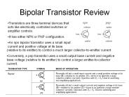
Bipolar Transistor Review Transistors are three terminal devices that acts like electrically controlled switches or amplifier controls. It has either NPN or PNP ...
| PowerPoint PPT presentation | free to download
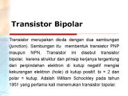
Transistor Bipolar Transistor merupakan dioda dengan dua sambungan (junction). Sambungan itu membentuk transistor PNP maupun NPN. Transistor ini disebut transistor ...
| PowerPoint PPT presentation | free to download

Definition An electronic device made of a semiconductor that can act as an insulator and a conductor. The ability to change from these two states enables the device ...
| PowerPoint PPT presentation | free to download

(transistor in saturation, no more linear relation between IC and IB) ... MOSFET s with temperature sensor High Electron Mobility Transistors (HEMTs) ...
| PowerPoint PPT presentation | free to view

Non-linear. Large variations in beta. Thermal runaway. Self-Bias Circuit ... thus reducing the effects of beta variations and temperature on the quiescent ...
| PowerPoint PPT presentation | free to view

chapter 2 transistors (BJT) 2.1 Transistor classification 2.2 Bipolar junction transistors (BJT) construction 2.3 Transistor action and operating 2.4 Quiescent ...
| PowerPoint PPT presentation | free to view

Introductions, trends in information technology; semiconductor physics, pn junction behavior, bipolar and MOS transistors, logic functions
| PowerPoint PPT presentation | free to download

FET Biasing The drain/source current raises the average channel voltage The effective gate voltage is then negative. ... (Lab - 02/01, Sat.) SCR s, ...
| PowerPoint PPT presentation | free to download

Describe the nature of both the base and collector characteristic curves for a BJT. ... 17. Base characteristic with collector-to-emitter voltage constant. ...
| PowerPoint PPT presentation | free to view

Field-effect transistors (FETs) EBB424E Dr. Sabar D. Hutagalung School of Materials & Mineral Resources Engineering, Universiti Sains Malaysia The Field Effect ...
| PowerPoint PPT presentation | free to download
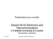
Transistors as a switch Session 6b for Electronics and Telecommunications A Fairfield University E-Course Powered by LearnLinc
| PowerPoint PPT presentation | free to download