
Transistors PowerPoint PPT Presentation
1 / 51
Title: Transistors
1
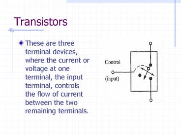
Transistors
- These are three terminal devices, where the
current or voltage at one terminal, the input
terminal, controls the flow of current between
the two remaining terminals.
2
Transistors
- Can be classified as
- FET Field Effect Transistor
- Majority carrier device
- Unipolar device
- BJT Bipolar Junction Transistor
- Minority carrier device
- Bipolar device.
3
FETs
- Two primary types
- MOSFET, Metal-Oxide-Semiconductor FET. Also known
as IGFET Insulated Gate FET - JFET, Junction FET.
- MOS transistors can be
- n-Channel
- Enhancement mode
- Depletion mode
- p-Channel
- Enhancement mode
- Depletion mode
4
MOSFET Structure
5
MOSFET
- MOSFETs are identified by symbols like the ones
shown below
6
MOSFET Operation
- Voltage at gate controls the flow of current
between drain and source. - VGS Voltage between gate and source.
- VDS Voltage between drain and source.
7
MOSFET Operation
- When VGS 0 then no current flows between drain
and source. - pn-Junction is reverse biased.
8
Threshold Voltage
- The value of VGS where the drain current just
begins to flow. - Typical values
- 0.3 to 0.8 volts.
9
MOSFET Operation
- Two cases
- Ohmic region
- Active Region
10
MOSFET Operation
- Ohmic Region
11
MOSFET Operation
- Active Region
12
K Parameter
- The constant K, called the conductance parameter,
is measured in units of mA/V2. - Where
13
MOSFET Output Curves
- A family of curves representing the V-I
characteristics of transistors. - A plot of drain current, ID, as a function of
drain-to-source voltage, VDS, for several values
of VGS.
14
Ohmic and Active Regions
15
P-Channel Enhancement MOSFET
- Note the n-type body and the p-type source and
drain areas. - Both VGS and VDD are negative with respect to
ground.
16
Depletion Mode MOSFETs
- n-Channel is built in.
- VGS varies from negative values to positive
values, where negative values of VGS depletes the
channel while positive values enhance it further.
17
JFETs
- Depletion-mode FET with a different structure
than that of the MOSFET. - Not generally used for switching elements of
digital circuits. - Used in special applications such as analog
circuits where very high input impedance is
required.
18
JFETs
- Every p-n junction has a depletion region devoid
of carriers, and the width of the depletion
region can be controlled by the applied voltage
across the junction.
19
JFETs
- Note the highest value of VGS.
- What happens if you make VGS positive with
respect to ground.
20
Inverter Circuit
- This circuit is designated as the common source
configuration. It is used in digital circuits.
21
Inverter Circuit
- When Vin is low the transistor is off and Vout is
high. - When Vin is high the transistor is on and Vout is
low.
22
MOSFET Circuit Model For Switching
- VGS controls the switch in the model and ron is
defined as
23
Inverter Circuit
24
Inverter Circuit
- For RL 1KO, and VDD5V.
25
Large Signal Amplifiers
- DC biasing
- Ensuring that the transistor has the correct dc
level at its terminals. - Termed as setting the Q-point, quiescent
operating bias point. - Same as setting the dc voltages and currents for
the circuit with no signal applied.
26
Large Signal Amplifiers
- The dc bias voltages and currents must be
maintained even when the circuit is confronted
with - Sources variations
- Temperature changes
- Change in component values due to manufacturing
process inconsistencies.
27
Common Source Amplifier
28
Common Source Amplifier
29
Self-Bias Circuit
- Useful for devices that require a negative
gate-to-source voltage (depletion mode n-channel
devices). - Negative gate-to-source voltages are achieved by
raising the source voltage higher than the gate
voltage.
30
Self-Bias Circuit
31
Self-Bias Circuit
32
Procedure
- Draw load line on the output curves of the
transistor. - Locate the Q-point on the load line.
- If there is a bypass capacitor in the circuit,
then construct an ac load line with slope - Calculate the large signal voltage gain.
33
Other FET Configurations
34
BJTs
- Invented in 1947 in the Bell Laboratories.
- It revolutionized electronics, by replacing the
vacuum tubes. - Standard for the TTL (Transistor-Transistor-Logic)
and ECL (Emitter-Coupled-Logic) families of
logic devices.
35
BJT Structure
- Three-layer sandwich of alternating semiconductor
materials. - Two types
- NPN
- PNP.
- Terminals
- Emitter
- Base
- Collector.
36
BJT Structure
- Two p n junction diodes built very close
together. - The junction between base and emitter is called
emitter junction, and the junction between base
and collector is called collector junction.
37
BJT Structure
- The emitter is placed on top of the collector
with a very thin base between them, and the
primary carrier flow is from the emitter to the
collector.
38
Modes of Operation
- Cutoff Both junctions are reverse biased and
the transistor appears as an open switch. - Saturation Both junctions are forward biased
and the transistor appears as a closed switch. - These two bias conditions are important for
digital circuits.
39
BJT Working as a Switch
- Note the simplified interpretation of the BJT
working as a switch in cutoff and saturation.
40
BJT Models for Switching
- IB(SAT) - the minimum base current to be exceeded
for the transistor to be considered in saturation
mode.
41
Modes of Operation
- Active The emitter junction is forward biased
and the collector junction is reverse biased. - Reverse active The emitter junction is reverse
biased and the collector junction is forward
biased.
42
Active Region
43
Active Region
44
Ebers-Moll Model
45
Ebers-Moll Model
46
Common Emitter Amplifier
47
Common Source Amplifier
- Non-linear.
- Large variations in beta.
- Thermal runaway.
48
Self-Bias Circuit
- Useful to control the effects discussed in the
previous slide. - This circuit stabilizes collector current instead
of base current, thus reducing the effects of
beta variations and temperature on the quiescent
operating point. - Collector current is determined by the voltage
across a resistor, RE, placed in series with the
emitter.
49
Self-Bias Circuit
50
Procedure
- Draw load line on the output curves of the
transistor. - Locate the Q-point on the load line.
- If there is a bypass capacitor in the circuit,
then construct an ac load line with slope - Calculate the large signal voltage gain.
51
Other BJT Configurations
Recommended
