
What You Will Learn In Next Few Sets of Lectures - PowerPoint PPT Presentation
1 / 45
Title:
What You Will Learn In Next Few Sets of Lectures
Description:
What You Will Learn In Next Few Sets of Lectures Basic CPU Architecture Single Cycle Data Path Design Single Cycle Controller Design Multiple Cycle Data Path Design – PowerPoint PPT presentation
Number of Views:79
Avg rating:3.0/5.0
Title: What You Will Learn In Next Few Sets of Lectures
1
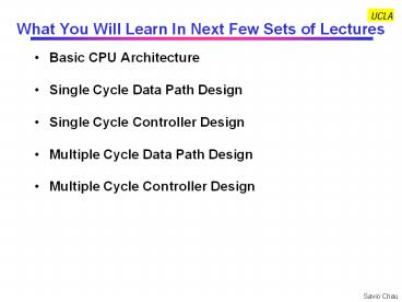
What You Will Learn In Next Few Sets of Lectures
- Basic CPU Architecture
- Single Cycle Data Path Design
- Single Cycle Controller Design
- Multiple Cycle Data Path Design
- Multiple Cycle Controller Design
Savio Chau
2
Five Classic Components of a Computer
- Todays Topic Designing a Single Cycle Datapath
3
The Processor
- Processor Executes The Program Instructions
- 2 Major Components
- Datapath
- Hardware to Execute Each Machine Instruction
- Consists of a cascade of combinational and state
elements (e.g., Arithmetic Logic Unit (ALU),
Shifters, Registers, Multipliers, etc.) - Control
- Generates the Signals Telling the Datapath What
To Do At Each Clock Cycle - Generates the Signals to Execute an Instruction
in a Single Cycle or as a Series of Small Steps
Over Multiple Cycles
4
A Simplified Processor Model
Memory
I/O
- Simplified Execution Cycle
- Instruction Fetch
- Instruction Decode
- Operand Fetch
- Execute
- Result Store
- Next Instruction
Data
Address
Control
Program Counter
Instruction Register
Control
Register File
ALU
Data Path
5
Execution Cycle
6
Steps to Design a Processor
- 5 steps to design a processor
- 1. Analyze instruction set
- Define the instruction set to be implemented
- Specify the requirements for the data path
- Specify the physical implementation
- 2. Select set of datapath components establish
clock methodology - 3. Assemble data path meeting the requirements
- 4. Analyze implementation of each instruction to
determine setting of control points that
effects the register transfer. - 5. Assemble the control logic
- MIPS makes it easier
- Instructions same size
- Source registers always in same place
- Immediates have same size, location
- Operations always on registers/immediates
Datapath Design
Cpntrol Logic Design
7
Step 1 Analyze the Instruction Seta) Defining
the Instruction Set Architecture
- Define the Functions of Each Instructions
- Data Movement load, store
- Arithmetic and Logic add, sub, ori, and, or, slt
- Program Control beq, jump
- For Each Instruction, Specify
- Instruction Mnemonics (Assembly Language)
- Instruction Format and Op Codes (Machine
Language)
8
Example Subset of MIPS ISA to be Implemented
9
Step 1 Analyze the Instruction Set b) Specify
Requirements for the Data Path
- Where and how to fetch the instruction?
- Where are the instructions stored?
- Instruction format or encoding
- how is it decoded?
- Location of operands
- where to find the operations?
- how many explicit operands?
- Data type and Size
- Type of Operations
- Location of results
- where to store the results?
- Successor instruction
- How to determine the next instruction?
- (next address logic for jumps, conditions
branches)
fetch-decode-execute next address is implicit!
10
Step 1 Analyze the Instruction Set c) Specify
the Physical Implementation
- Write Register Transfer Language (RTL) for the
ISA - Specify what state elements (registers, memories,
flip-flops) are needed to implement the
instructions - Describe how signals are transferred among state
elements - There are many types of RTLs. Examples VDHL and
Verilog - An informal RTL is used in this class
- Syntax
- variable ? expression
- Where variable is either a register or a signal
or signal group - (Note Use the following convention in this
class. - Variable is a register if it is all caps or in
form of arrayaddress. Otherwise it is a
signal or signal group) - Expression is a function of input signals and
the output of other state elements
11
RTL Conventions for This Class
- Register names Either all upper case,
underlined, or in array format. Examples - REG all upper case
- Reg not all upper case but underlined
- Reg10 10th register in a register file
- Signal names or signal group names neither all
upper case nor underlined. Examples - Output
- output
- Register transfers
- A ? B register to register
- REG ? input signal to register
- Each register write statement is assumed to take
one clock unless is grouped by . Register
read doesnt take any clock. Examples - A ? B reg to reg A ? B reg to reg a
? B reg to signal - C ? A C ? A c ? A
- Takes 2 clocks. Write Takes 1 clock. Write Takes
0 clock. Read - transfers are sequential transfers are in
parallel transfer is immediate
REG
input
output
clock
12
Register Transfer in RTL
RTL B can also be written as A ? A B
AOut ? A B B ? (A B) xor C XOut ? AOut
xor C C ? B B ? XOut
13
RTL Bit Level Description
Use pointed bracket to denote the bits in a
register or signal group, e.g., Alt 31 0gt means
bit 31 to bit 0 of register A
F ? Elt26 23gt E ? E SignExtend( F) Another
way of expressing Alternatively Flt3gt ? Elt26gt
Flt3 0gt ? Elt26 23gt Flt2gt ? Elt25gt Flt1gt ?
Elt24gt Flt0gt ? Elt23gt
14
RTL Memory Description
Memory is described as an array General
purpose registers are described as an array e.
g., Mem100 Contents of address 100 in
memory R6 Contents of Register 6 Rrs
Contents of the register whose register
number is specified by the signal rs
15
RTL Conditionals
Conditionals can also be used in RTL e. g.,
RTL if (Select 0) then Output ?
Input_0 else if (Select 1) then Output ?
Input_1
16
Register Transfer Language and Clocking
Register transfer in RTL
R2 ? f(R1)
What Really Happens Physically
0
1
1
1
1
0
0
1
1
1
Two possible clocking methodologies positively
triggered or negatively triggered. This class
uses the negatively-triggered.
17
Instructions and RTLfor the MIPS Subset
- RTL
- instr ? memPC Instruction Fetch
- rs ? instrlt2521gt Define Signals (Fields) of
Instr - rt ? instrlt2016gt
- rd ? instrlt1511gt
- Rrd ? Rrs Rrt Add Register Contents
- PC ? PC 4 Update Program Counter
RTL Instr ? memPC Instruction Fetch rs ?
instrlt25 21gt Define Signals (Fields) of
Instr rt ? instrlt20 16gt rd ? instrlt15 11gt Rrd
? Rrs - Rrt Subtract Register Contents PC ?
PC 4 Update Program Counter
18
Instructions and RTLfor the MIPS Subset
(continued)
- RTL
- instr ? memPC Instruction Fetch
- rs ? instrlt2521gt Define Signals (Fields) of
Instr - rt ? instrlt2016gt
- imm16 ? instrlt150gt
- addr ? Rrs sign_extend(imm16) Calculate
Memory Address - Rrt ? Memaddr Load Data into Register
- PC ? PC 4 Update Program Counter
19
Instructions and RTLfor the MIPS Subset
(continued)
- RTL
- instr ? memPC Instruction Fetch
- rs ? instrlt2521gt Define Signals (Fields) of
Instr - rt ? instrlt2016gt
- imm16 ? instrlt150gt
- addr ? Rrs sign_ext(imm16) Calculate Memory
Address - Memaddr ? Rrt Store Register data Into
Memory - PC ? PC 4
RTL instr ? memPC Instruction Fetch rs ?
instrlt2521gt Define Signals (Fields) of Instr rt
? instrlt2016gt imm16 ? instrlt 15 0gt Rrt ?
Rrs or zero_ext(imm16) Logical OR PC ? PC 4
Update Program Counter
20
Instructions and RTLfor the MIPS Subset
(continued)
- RTL
- instr ? memPC Instruction Fetch
- rs ? instrlt2521gt Define Signals (Fields) of
Instr - rt ? instrlt2016gt
- imm16 ? instrlt150gt
- branch_ cond ? Rrs - Rrt Calculate Branch
Condition - if (branch_cond eq 0) Calculate Next Instruction
Address - then PC ? PC 4 (sign_ext(imm16) 4)
- else PC ? PC 4
RTL instr ? memPC Instruction Fetch PC_incr ?
PC 4 Increment Program Counter PClt312gt ?
PC_incrlt3128gt concat targetlt250gt Calculate
Next Instr. Addr. Note PClt 1 0gt is 00 for a
word address so not necessary to implement PClt 1
0gt
21
Step 2 Select Basic Processor Elements
Possible Elements to be Used in Data Path
22
Data Path Element Example ALU
23
Data Path Element Example Register File
Clock Signal
24
Implementation of Register File
clock
25
Data Path Element Example An Idealized Memory
26
Step 3 Assemble the Datapath Put Together a
Datapath for R-Type Instruction
- General format Op rd, rs, rt
- (e.g., add rd, rs, rt)
- instr ? memPC Instruction Fetch
- rs ? instrlt2521gt Define Signals (Fields) of
Instr - rt ? instrlt2016gt
- rd ? instrlt1511gt
- Rrd ? Rrs Rrt Add Register Contents
- PC ? PC 4 Update Program Counter
Next Address Logic
PC
rs
Instruction Memory
Register File
Rd addr1
rt
Rd addr2
rd
Wr addr
Wr data
See Example Before Animating the Construction of
the Data Path
27
Step 3 Assemble the DatapathDetails of
Instruction Fetch Unit
- The Common RTL Operations
- Fetch the Instruction and Define signal fields of
the instruction - instr ? mem PC rs ? instrlt 25 21gt rt ?
instrlt 20 16gt - rd ? instrlt 15 11gt imm16 ? instrlt 15 0gt
- Update the Program Counter
- Sequential Code PC ? PC 4
- Branch and Jump PC ? something else
To Data Path
28
Operations of R-Type Instruction Datapath
R rd ? R rs op R rt Example add rd, rs,
rt instr ? memPC Instruction Fetch rs ?
instrlt2521gt Define Signals (Fields) of
Instr rt ? instrlt2016gt rd ?
instrlt1511gt Rrd ? Rrs Rrt Add Register
Contents PC ? PC 4 Update Program
Counter ALUctr and RegWr Control Signals from
Control Logic
Instruction Memory
PC
rd
29
Details of R-Type Instruction Timing
Clk to-Q
Old Value
New Value
Instruction Memory Access Time
Old Value
New Value
Delay Through Control Logic
Old Value
New Value
Control Signal
Old Value
New Value
Control Signal
Register File Access Time
Old Value
New Value
ALU Delay
Old Value
New Value
30
Step 3 Assemble the Datapath (continue) Put
Together a Datapath for Load Instruction
- lw rt, immed16(rs)
- Instr ? memPC Instruction Fetch
- rs ? Instrlt2521gt Define Signals (Fields) of
Instr - rt ? Instrlt2016gt
- imm16 ? Instrlt150gt
- Addr ? Rrs SignExtend(imm16) Calculate
Memory Address - Rrt ? MemAddr Load Data into Register
- PC ? PC 4 Update Program Counter
Next Address Logic
PC
rs
Instruction Memory
Register File
Rd addr1
rt
imm16
Wr addr
Wr data
ext
See Example Before Animating the Construction of
the Data Path
31
Operations of the Datapath for Load Instruction
R rt ? Mem R rs SignExt( imm16)
Example lw rt, imm16( rs)
Instruction Memory
PC
rs
rt
data
32
Timing of a Load Instruction
Clk to-Q
Old Value
New Value
Instruction Memory Access Time
Old Value
New Value
Delay Through Control Logic
Old Value
New Value
Old Value
New Value
Old Value
New Value
RegWr busA busB Address busW
Old Value
New Value
Register File Access Time
Old Value
New Value
Delay through Extender Mux
Old Value
New Value
ALU Delay
Old Value
New Value
Data Memory Access MUX Time
Old Value
New Value
33
Step 3 Assemble the Datapath (continue) Put
Together a Datapath for Store Instruction
- sw rt, immed16(2)
- Instr ? memPC Instruction Fetch
- rs ? Instrlt2521gt Define Signals (Fields) of
Instr - rt ? Instrlt2016gt
- imm16 ? Instrlt150gt
- Addr ? Rrs SignExt(imm16) Calculate Memory
Address - MemAddr ? Rrt Store Register data Into
Memory - PC ? PC 4
Next Address Logic
PC
rs
Instruction Memory
Register File
Rd addr1
rt
Rd addr2
imm16
ext
34
Operations of the Datapath for Store Instruction
Instruction Memory
PC
memrt
35
Step 3 Assemble the Datapath (continue) Put
Together a Datapath for I-Type Instruction
- General format Op rt, rs, immed16
- (e.g., ori rt, rs, immed16)
- Instr ? memPC Instruction Fetch
- rs ? Instrlt2521gt Define Signals (Fields) of
Instr - rt ? Instrlt2016gt
- imm16 ? Instrlt150gt
- Rrt ? Rrs or ZeroExt(imm16) Logical OR
- PC ? PC 4 Update Program Counter
PC4
Next Address Logic
PC
rs
Register File
Instruction Memory
Rd addr1
rt
imm16
Wr addr
Wr data
ext
36
Operations of the I-Type Instruction Datapath
Rrt ? Rrs op ZeroExt(lmm16) op , -,
and, or etc. Example ori rt, rs, Imm16
Instruction Memory
PC
rs
rt
37
Step 3 Assemble the Datapath (continue) Put
Together a Datapath for Branch Instruction
- beq rs, rt, immed16
- Instr lt- memPC Instruction Fetch
- rs lt- Instrlt2521gt Define Signals (Fields) of
Instr - rt lt- Instrlt2016gt
- imm16 lt- Instrlt150gt
- branch_ cond lt- Rrs - Rrt Calculate Branch
Condition - if (branch_ cond eq 0) Calculate Next
Instruction Address - then PC lt- PC 4 (SignExt(immd16) 4)
- else PC lt- PC 4
Next Address Logic
PC
rs
Instruction Memory
Register File
Rd addr1
rt
Rd addr2
imm16
ext
38
Step 3 Assemble the Datapath (continue)
Combining Datapaths for Different Instructions
- Example Combining Data Paths for add and lw
See Example Before Animating the Construction of
the Data Path
39
Operations of the Datapath for Branch Instruction
Instruction Memory
Pc4 imm16
PC4
40
Binary Arithmetic for the Next Address
- In Theory, the PC is a 32- bit byte Address Into
the Instruction Memory - Sequential Operation PClt 31 0gt PClt 31 0gt 4
- Branch Operation PClt 31 0gt PClt 31 0gt 4
SignExt( Imm16) 4 - The Magic Number 4 Always Comes Up Because
- The 32- Bit PC is a Byte Address
- And All Our Instructions are 4 Bytes (32- bits)
Long - In Other Words
- The 2 LSBs of the 32- bit PC are Always Zeros
- There is No Reason to Have Hardware to Keep the 2
LSBs - In Practice, We Can Simplify the Hardware by
Using a 30- bit PClt 31 2gt - Sequential Operation PClt 31 2gt PClt 31 2gt 1
- Branch Operation PClt 31 2gt PClt 31 2gt 1
SignExt(imm16) - In Either Case, Instruction Memory Address PClt
31 2gt concat 00
41
Next Address Logic Including Branch Instructions
1 MUX delay after branch decision is made
42
Next Address Logic Cheaper Solution
1 MUX 1 Adder delay after branch decision is
made
43
A Complete Instruction Fetch Unit
Question What is the data path for Jump
instruction? Answer None. Jump instruction is
handled by Instruction Fetch Unit alone.
44
Putting It All Together A Single Cycle Datapath
45
Load Instruction in the Complete Data Path
rs
PC4
data for rt