
Chapter 8: Hybrid Technology and Multichip Modules PowerPoint PPT Presentation
1 / 64
Title: Chapter 8: Hybrid Technology and Multichip Modules
1
Chapter 8 Hybrid Technology and Multichip Modules
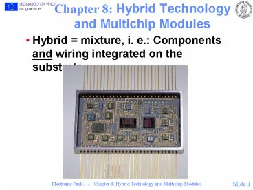
- Hybrid mixture, i. e. Components and wiring
integrated on the substrate
2
Types of Hybrids and Multichip Modules
- Thick film technology
- High temperature thick film hybrid technology
- Polymer thick film hybrid technology
- Thin film technology
- Conventional thin film technology (one conductor
layer) - Multilayer thin film technology
- Multichip modules
- Multilayer ceramic (MCM-C) (C for ceramic)
- Multilayer thin film (MCM-D) (D for deposited)
- Multilayer fineline circuit boards (MCM-L) (L for
laminated) Please also confer to Chapter 5.
3
High Temperature Thick Film Technology
- Important substrate properties
- Dimensional stability
- Good adhesion
- High thermal conductivity
- Thermal compatibility with components
- High electrical resistivity
- Low dielectric constant (not satisfied in
alumina) - Low dielectric loss tangent
- Good machinability (not satisfied in ceramics)
- Low price
4
High Temp Thick Film, continued
- Practical materials
- Alumina
- Aluminium nitride
- (Beryllia)
- (Silicon carbide)
- Table 8.1Properties of substrate materials for
hybrid technology.P Plastic In Insulator
5
Conductor Materials
- Composition
- Functional element (metal paticles)
- Binder (glass particles)
- Solvents
- Desired properties
- High electrical conductivity
- Good adhesion to substrate
- Good solderability
- Good bondability
- Low price
6
Conductor Materials, continued
- Practical functional element
- Gold
- Ag/Pd
- Ag/Pt
- Copper
Table 8.2 Properties of thick film conductor
systems
7
Thick Film Resistors
- Important properties
- Large range of resistor values
- High stability
- Low thermal coefficient of resistivity
- Low voltage coefficient of resistivity
- Low noise
- Materials
- Oxides of ruthenium
- Oxides of iridium, rhodium, osmium
- Sheet resistance 1 - 109 ohms/sq
8
Properties of Thick Film Resistors
- Table 8.3 Typical properties of thick film
resistors.
9
Termination of Thick Film Resistors
- Fig. 8.2 Thick film resistor with termination
10
Insulators / Dielectrics
- Desired properties
- High insulation resistance
- High breakdown field
- Low dielectric constant (insulation)
- Suitable/high dielectric constant (dielectric)
- Low temperature coefficient (dielectric)
- Low voltage coefficient (dielectric)
- Low loss tangent
- Little porosity
11
Insulators / Dielectrics, continued
- Materials
- Aluminium oxide/glass (insulator)
- Ceramics/glasses as for capacitors (dielectric)
- Please also see Chapter 4
12
Insulators / Dielectrics, continued
- Table 8.4 Typical properties of printed and
discrete capacitors.
13
Production Process for High Temperature Thick
Film Technology
- Layout and photolithographics
- CAD work
- Photo or laser plotting of master films
- Printing screens made with master films
14
Production process, continued
- Printing process
- Printing
- Drying at 100 - 150 C
- Firing at 700 - 1000 C
- Fig 8.1 Typicaltemperature profilefor thick
filmfiring.
15
Production process, continued
- Testing and laser trimming
- Initial value targeted 20 - 30 below specified
value - Laser trimming to increase resistance within
0.5 or 1.0
Fig. 8.4 Probe card for testing of thick- and
thin film hybrid circuits. Coaxial probes are
used for high frequency signals.
16
Laser trimming
a)
b)
c)
- Fig. 8.5 Laser trim cut forms a) L-cut, the
most common b) Top hat plunge cut c) Digital
trimming, which is most used for high precision
thin film resistors
17
Laser trimming, continued
- Fig. 8.6 Laser trimmer for thick film hybrid
circuits, ESI Model 44.
18
Production process, continued
- Fig. 8.7 Process flow for mounting of thick film
hybrid circuits based on a) Naked ICs and
gluing of discrete components.
19
Production process, continued
- Fig. 8.7 Process flow for mounting of thick film
hybrid circuits based on b) Soldering of
packaged ICs and discrete components.
20
Polymer Thick Film Technology
- In polymer thick film hybrid technology (PTF)
conductors, resistors and insulating layers use a
polymer matrix instead of glass matrix, and these
are made in several layers on ordinary printed
wiring board laminates, flexible substrates and
injection moulded plastic materials that can
serve as combined printed circuits and chassis.
21
Polymer Thick Film, continued
- Advantages
- Low price
- Simple processes
- Fast production throughput
- Well suited for repair/modification
- Printed resistors possible
- Additive technology
- Printed wiring boards for substrates
- Specialities
- Membrane switch panels
- Contacts
22
Polymer Thick Film, continued
- Limitations
- Satisfies only moderate environmental
requirements - Low/moderate complexity
- High sheet resistivity in conductors
- Special design rules
- Limited solderability
- Limited shelf life for pastes
- Limited availability
23
Polymer Thick Film, continued
- Fig. 8.8 Polymer Thick film (PTF) carbon
technology, for - a) Keyboard contacts.
- b) Contacts of LCD- displays.
- c) Sliding potentiometer.
- CPTF means carbon type PTF.
24
Polymer Thick Film, continued
- Materials
- Matrix Thermosetting /thermoplastic polymer
- Conductor Ag, Cu, C
- Solvents
- Additives to adjust consistency
- Ceramic or other additives
25
Polymer Thick Film, continued
- A typical process
- The starting material is a laminate with a single
sided etched conductor pattern in Cu foil - 1. Cleaning of the board
- 2. Printing of PTF insulation layer, 2 prints,
drying in between - 3. Drying
- 4. UV curing
- 5. Printing of PTF conductor
- 6. Drying
- 7. Curing in IR in-line furnace
- 8. Chemical plating of metal (Optional)
- 9. Printing of top layer
- 10. Drying
- 11. Curing in IR furnace.
26
Polymer Thick Film, continued
- Fig. 8.9 Membrane switch panel, principle.
27
PTF, continued
- Fig. 8.10 PTF based printed wiring boards a)
Single sided board with PTF for one complete
conductor layer on top of one Cu foil conductor
plate. b) Double sided, through hole plated
board with one extra PTF conductor layer on each
side. c) Double sided board through hole
printed PTF conductor, instead of through hole
plating.d) PTF resistor
28
Thin Film Technology
- Substrate materials
- Alumina, glass, silicon
- Conductor materials
- Gold, aluminium
- Resistor materials
- NiCr (Chromnickel), Ta2N (Tantalnitrid)
- Insulation/dielectrics/passivation materials
- SiO2 (Silicon dioxide), SiN3 (Silicon nitride),
Al2O3 (Silicon nitride), Ta2O5 (Tantaloxide)
29
Thin Film Technology, continued
- Table 8.5 Properties of thin film resistors.
(d skin depth. Evap Vacuum evaporation. Sp
Sputtering)
30
Thin FilmProcessing
- Photolithography and etching
- Vacuum evaporation
- Sputtering
- Plating
- Oxidation
- Fig. 8.11 Process flow for production of thin
film hybrid circuits.
31
Thin Film Processing, continued
- Fig. 8.12 Structure of thin film resistor with
gold termination.
32
Thin Film Processing, continued
- Fig. 8.13 Thin film microwave circuit,
schematically.
33
Thin Film Processing, continued
- Fig. 8.14 Thin film transistors, structure.
34
Thin Film Processing, continued
- Circuit production
- Glueing
- Wire bonding
- Testing
- Packaging in hermetic (metal) box
35
Multilayer Thin Film - MCM-D
- Process
- 1. Spinning polyimide insulation
- 2. Deposition Al metallization
- 3. Photolithography, wet etch
- 4. Spinning polyimide
- 5. Etching vias
- 6. Repetition steps 1 - 5
- 7. Metallization and etching of metal
36
MCM-D, continued
- Fig. 8.15 a) ATTs structure for multilayer
thin film. Please also see also Figure 2.13.
37
MCM-D, continued
- Fig. 8.15 b) Cross section of Raychems High
Density Interconnect (HDI) schematically and
observed through microscope.
38
MCM-D, continued
- Fig. 8.16 Elements of the design rules for
Raychems HDI technology
39
MCM-D, continued
- Fig. 8.17 Characteristic impedance for Raychems
HDI as function of the ratio between conductors
width and dielectric thickness.
40
MCM-D, continued
- Fig. 8.18a) Dissipation factor for Raychems
HDI
41
MCM-D, continued
- Fig. 8.18. b)Typical attenuation, as function
of frequency, for Raychems HDI. Even at 10 GHz
attenuation in the conductor metal dominates.
42
MCM-D, continued
- Advantages
- Optimal thermal match when Si substrate
- High thermal conductivity in Si 150 W/C x m
- Termination resistors and decoupling capacitors
integrated in substrate - Compatibility with
- Wire bonding
- TAB
- Flip chip
- Very high conductor density/package density
- Very good high frequency properties
- Good mechanical properties of Si substrate
- High reliability
43
MCM-D, continued
- Disadvantages
- Low availability and high cost
- Polyimide is hygroscopic
- Important properties change
- Reliability problems
- Hermetic encapsulation necessary
- Immature technology
44
Multilayer Ceramic Modules - MCM-C
- Materials
- Alumina
- Aluminium nitride
- Pioneer IBM
- Fabrication Green Tape process
45
MCM-C, continued
- Fig. 8.19 Production process for multilayer
ceramic, schematically.
46
MCM-C, continued
- Advantages
- High thermal conductivity
- Low TCE, match to Si, GaAs, SMDs
- Compatible to flip chip, wire bonding, TAB, SMD
soldering - Control over characteristic impedance
- Hermetic encapsulation possible, high reliability
- Many conductor layers, high yield
- Edge contacts, etc. brazed on
47
MCM-C, continued
- Disadvantages
- Low electrical conductivity in inner layers (Rsq
15 mOhm/sq) - High dielectric constant, ?r 9 - 10
- High startup cost for custom specific circuits
48
MCM-C, continued
- Fig. 8.20 Combination of naked chips in cavities
and soldered, packaged SMD components on
multilayer ceramic module
49
MCM-C, continued
- Fig. 8.21.a Characteristic impedance for
typical geometries and dimensions, Al2O3-based
multilayer ceramic a) Open microstrip.
50
MCM-C, continued
- Fig. 8.21.b Characteristic impedance for
typical geometries and dimensions, Al2O3-based
multilayer ceramic b) Buried microstrip.
51
MCM-C, continued
- Fig. 8.21.c Characteristic impedance for
typical geometries and dimensions, Al2O3-based
multilayer ceramic c) Stripline.
52
MCM-C, continued
- Table 8.6 Properties of alumina-based high
temperature multilayer ceramic.
53
Low Temperature Multilayer Ceramic Modules -
LTMCM-C
- Substrate materials
- Glasses, glass ceramics
- Mullite, corderite, lead borosilicate glass...
- Conductors
- Gold, silver, AgPd
- Resistors
- Similar to thick film
- Properties Table 8.7.
54
LTMCM-C, continued
- Table 8.7 Electrical and physical properties of
low temperature multilayer ceramic. a)
Electrical properties.
55
LTMCM-C, continued
- Table 8.7 Electrical and physical properties of
low temperature multilayer ceramic. b) Resistor
Performance - Resistance and TCR.
56
LTMCM-C, continued
- Table 8.7 Electrical and physical properties of
low temperature multilayer ceramic. c) Physical
properties.
57
LTMCM-C, continued
- Advantages
- Low process temperature
- Most process steps can be done in high
temperature thick film production line - Flexibility in conductor materials, low sheet
resistivity - Plating not necessary for bonding
- Screen printed resistors
- Low er dielectric materials
58
LTMCM-C, continued
- Disadvantages
- New, immature technology
- Low thermal conductivity
- Brittle materials
- Low availability
59
Power Electronic Modules
- Challenges
- Spread the heat, reduce thermal resistance
- Reduce thermal stress
- Provide electrical insulation for 2.5 kV
- Design for EMC, reduce L
- Higher integration "smart power
60
Power Electronic Modules, continued
- Technologies
- Polymer on metal
- Thick film
- Plated ceramic substrate
- Direct copper bonding (DCB)
- Plasma sprayed dielectric on metal base
- Direct Copper Bonding
61
Power Electronic ModulesDirect Copper Bonding
- Fig. 8.22 a) The coefficient of thermal
expansion for direct copper bonding (DCB)
substrates with a layer of 0,6 mm alumina
sandwiched between Cu layers of various
thicknesses as given in the figure.b) The
number of thermal cycles to fracture for DCB
substrates with varies Cu thickness. The cycles
were in the temperature interval -40 - 110C.
62
Direct Copper Bonding, continued
- Fig. 8.23 Power electronic module Toshiba data
sheet. The substrate (top) is DCB with AlN
insulation. It is soldered to a heavy Cu plate,
environmentally protected with silicone gel and
mounted in a plastic package with heavy screw
terminals. Each of the transistor chips and diode
chips conducts up to 50 A current.
63
Combination Technologies
- Multilayer thin film - on - multilayer ceramic
- Fig. 8.24 High performance modules made in a
combination of multilayer thin film and multi
layer ceramic technology a) NEC Corporation
computer SX-3 using flop TAB carrier on thin film
and alumina based substrate. b) IBM Enterprise
System/9000 packaging hierarchy using flip chip,
polyimide/copper thin film on 63 layers glass
ceramic substrate.
a)
b)
64
Combination Technologies, continued
- Thin film - on - thick film (ame, Horten).
Fig.8.25
1. Alumina substrate. 2.a,b,c,d Printed
conductor on first layer. 3. Printed dielectric
film. 4. Optional compensation printed in
vias. 5.a,b,c Printed conductor on second
layer. 6. Glass based dielectric. 7. a,b,c,d
Tantalum nitride resistive layer.
8.a,b,c,d Molybdenum diffusion barrier. 9.a,b,c
Thin film gold lines. 10. Via hole between thin
film and thick film conductive layer. 11.
Contact area in thick film. Gold- platinum
or gold-palladium. 12.a,b Resistor in thin film
made by selective etching in thin film
structure
Recommended
