
Ultra-Scaled MOSFETs for Future Nanoelectronics PowerPoint PPT Presentation
1 / 21
Title: Ultra-Scaled MOSFETs for Future Nanoelectronics
1
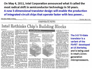
On May 4, 2011, Intel Corporation announced what
it called the most radical shift in semiconductor
technology in 50 years. A new 3-dimensional
transistor design will enable the production of
integrated-circuit chips that operate faster with
less power
The 3-D Tri-Gate transistor is a variant of the
FinFET developed at UC-Berkeley, and is being
used in Intels 22nm-generation microprocessors.
2
Lecture 24
- OUTLINE
- The MOSFET (contd)
- Advanced MOSFET structures
- Reading Hu 7.8
3
Why New Transistor Structures?
- Off-state leakage (IOFF) must be suppressed as Lg
is scaled down - allows for reductions in VT and hence VDD
- Leakage occurs in the region away from the
channel surface - ? Lets get rid of it!
Lg
Drain
Source
3
4
Thin-Body MOSFETs
- IOFF is suppressed by using an adequately thin
body region. - Body doping can be eliminated
- ? higher drive current due to higher carrier
mobility
Ultra-Thin Body (UTB)
Double-Gate (DG)
Lg
Source
Drain
TSi
TSi
Source
Drain
Buried Oxide
Substrate
TSi lt (1/4) ? Lg
TSi lt (2/3) ? Lg
4
5
Effect of TSi on OFF-state Leakage
Lg 25 nm tox,eq 12Å
TSi 10 nm
TSi 20 nm
106
3x10²
10-1
Leakage Current Density A/cm2 _at_ VDS 0.7 V
IOFF 19 ?A/?m
IOFF 2.1 nA/?m
5
6
Double-Gate MOSFET Structures
PLANAR
VERTICAL
FINFET
L. Geppert, IEEE Spectrum, October 2002
6
7
DELTA MOSFET
D. Hisamoto, T. Kaga, Y. Kawamoto, and E. Takeda
(Hitachi Central Research Laboratory), A fully
depleted lean-channel transistor (DELTA) a
novel vertical ultrathin SOI MOSFET, IEEE
Electron Device Letters Vol. 11, pp. 36-39, 1990
- Improved gate control observed for Wg lt 0.3 mm
- LEFF 0.57 mm
Wl 0.4 mm
7
8
Double-Gate FinFET
- Self-aligned gates straddle narrow silicon fin
- Current flows parallel to wafer surface
Gate Length Lg
Source
Gate 2
Gate 1
Current Flow
Drain
Fin Height Hfin W
Fin Width Wfin TSi
8
9
1998 First n-channel FinFETs
D. Hisamoto, W.-C. Lee, J. Kedzierski, E.
Anderson, H. Takeuchi, K. Asano, T.-J. King, J.
Bokor, and C. Hu, A folded-channel MOSFET for
deep-sub-tenth micron era, IEEE International
Electron Devices Meeting Technical Digest, pp.
1032-1034, 1998
Plan View
Lg 30 nm Wfin 20 nm Hfin 50 nm
Lg 30 nm Wfin 20 nm Hfin 50 nm
- Devices with Lg down to 17 nm were successfully
fabricated
9
10
1999 First p-channel FinFETs
X. Huang, W.-C. Lee, C. Kuo, D. Hisamoto, L.
Chang, J. Kedzierski, E. Anderson, H. Takeuchi,
Y.-K. Choi, K. Asano, V. Subramanian, T.-J.
King, J. Bokor, and C. Hu, Sub 50-nm FinFET
PMOS, IEEE International Electron Devices
Meeting Technical Digest, pp. 67-70, 1999
Lg 18 nm Wfin 15 nm Hfin 50 nm
Transmission Electron Micrograph
10
11
UC-Berkeley FinFET Patent
27 additional claims
11
12
2001 15 nm FinFETs
Y.-K. Choi, N. Lindert, P. Xuan, S. Tang, D. Ha,
E. Anderson, T.-J. King, J. Bokor, C. Hu,
"Sub-20nm CMOS FinFET technologies, IEEE
International Electron Devices Meeting Technical
Digest, pp. 421-424, 2001
Transfer Characteristics
Output Characteristics
Wfin 10 nm Tox 2.1 nm
12
13
2002 10 nm FinFETs
B. Yu, L. Chang, S. Ahmed, H. Wang, S. Bell,
C.-Y. Yang, C. Tabery, C. Hu, T.-J. King, J.
Bokor, M.-R. Lin, and D. Kyser, "FinFET scaling
to 10nm gate length," International Electron
Devices Meeting Technical Digest, pp. 251-254,
2002
SEM image
TEM images
- These devices were fabricated at AMD, using
optical lithography.
13
14
Tri-Gate FET (Intel Corp.)
Lg 60 nm Wfin 55 nm Hfin 36 nm
B. Doyle et al., IEEE Electron Device Letters,
Vol. 24, pp. 263-265, 2003
14
15
Bulk FinFET (Samsung Electronics)
- FinFETs can be made on bulk-Si wafers
- lower cost
- improved thermal conduction
- 90 nm Lg FinFETs demonstrated
- Wfin 80 nm
- Hfin 100 nm
- DIBL 25 mV
C.-H. Lee et al., Symposium on VLSI Technology
Digest, pp. 130-131, 2004
15
16
2004 High-k/Metal Gate FinFET
D. Ha, H. Takeuchi, Y.-K. Choi, T.-J. King, W.
Bai, D.-L. Kwong, A. Agarwal, and M. Ameen,
Molybdenum-gate HfO2 CMOS FinFET technology,
IEEE International Electron Devices Meeting
Technical Digest, pp. 643-646, 2004
16
17
Impact of Fin Layout Orientation
L. Chang et al. (IBM), SISPAD 2004
- If the fin is oriented or ? to the wafer flat,
the channel surfaces lie along (110) planes. - Lower electron mobility
- Higher hole mobility
- If the fin is oriented 45 to the wafer flat, the
channel surfaces lie along (100) planes.
(Series resistance is more significant at shorter
Lg.)
17
18
May 4, 2011 Intel Announcement
- Ivy Bridge-based Intel Core family processors
will be the first high-volume chips to use 3-D
Tri-Gate transistors. - This silicon technology breakthrough will also
aid in the delivery of more highly integrated
Intel Atom processor-based products
18
http//newsroom.intel.com/community/intel_newsroom
/blog/2011/05/04/intel-reinvents-transistors-using
-new-3-d-structure
19
22 nm node Tri-Gate FETs
- Lg 30-34 nm Wfin 8 nm Hfin 34 nm
- High-k/metal gate stack, EOT 0.9 nm
- Channel strain techniques
Transfer Characteristics
IOFF vs. IEFF
IOFF vs. IEFF
NMOS
PMOS
C. Auth et al., Symp. VLSI Technology 2012
19
20
National Science Foundation (NSF) Science and
Technology Center (STC) for Energy Efficient
Electronics Science PI Eli Yablonovitch (UC
Berkeley) 10-yr project, started 15 Sep 2010
Goal Develop a new switch that can operate with
VDD 1 mV
- Theme I Nanoelectronics (Prof. Eli
Yablonovitch) - Theme II Nanomechanics (Prof. Tsu-Jae King Liu)
- Theme III Nanomagnetics (Prof. Jeffrey Bokor)
- Theme IV Nanophotonics (Prof. Ming Wu)
Contra Costa-UC Berkeley-MIT-LATTC-Stanford-Tuskeg
ee
20
21
A Vision of the Future
Investment
Market Growth
- Information technology will be
- pervasive
- embedded
- human-centered
- solving societal
- scale problems
21
Recommended
