
Amorphous Si photonic devices PowerPoint PPT Presentation
1 / 1
Title: Amorphous Si photonic devices
1
Amorphous Si photonic devices
Laboratory of Optics, Photonics and Quantum
Electronics Dept. of Microelectronics and Applied
Physics Royal Institute of Technology, Stockholm,
Sweden
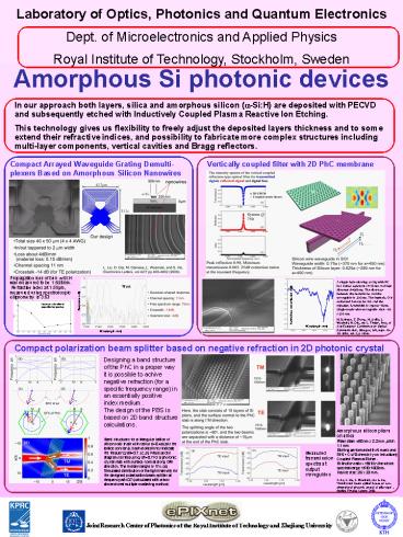
In our approach both layers, silica and amorphous
silicon (a-SiH) are deposited with PECVD and
subsequently etched with Inductively Coupled
Plasma Reactive Ion Etching. This technology
gives us flexibility to freely adjust the
deposited layers thickness and to some extend
their refractive indices, and possibility to
fabricate more complex structures including
multi-layer components, vertical cavities and
Bragg reflectors.
Compact Arrayed Waveguide Grating Demulti-plexers
Based on Amorphous Silicon Nanowires
Vertically coupled filter with 2D PhC membrane
Propagation loss of bulk a-SiH was measured to
be 1.5dB/cm. Refractive index at 1.55µm,
measured using spectroscopic ellipsometry is 3.63
A single hole missing cavity with PC has lattice
constant a480nm and hole diameter d289nm. The
distance between the membrane and the waveguide
is 250 nm. The intrinsic Q is estimated here to
be 500 and the rejection bandwidth is approx
10nm. Single mode wire waveguide size 400 x 250
nm. M. Dainese, Z. Zhang, M. Swillo, L. Wosinski,
M. Qiu, and L. Thylén, Proc. of 31st European
Conference on Optical Communication, Glasgow, UK,
Sept. 25-29. 2005, vol. 2, p 185-6.
Normalized transmission (dB)
Losses as a function of deposition temperature
Wavelength (nm)
Compact polarization beam splitter based on
negative refraction in 2D photonic crystal
Designing a band structure of the PhC in a proper
way it is possible to achive negative refraction
(for a specific frequency range) in an
essentially positive index medium. The design of
the PBS is based on 2D band structure
calculations.
Amorphous silicon pilars on silica Pilars diam
450 nm x 2.2 mm, pitch 1.1 mm Etching performed
with Al mask and SF6 C4F8 chemistry on
Inductively Coupled Plasma Etcher. Extinction
ratio 15dB in the whole spectral range
1510-1600nm. Device size 26 x 20 mm. X. Ao, L.
Liu, L. Wosinski, and S. He, Polarization beam
splitter based on two-dimensional photonic
crystal of pillar type , Applied Physics Letters
2006.
Band structures for a triangular lattice of
silicon rods in air with radius d0.4a (a is the
lattice constant). Dash-dotted lines indicate the
frequency a/l0.7. (c, d) Wave vector diagrams at
frequency a/l0.7 for a photonic crystal slab
with surface normal along GM direction. The
incident angle is 17o. (e) Simulated distribution
of the light intensity for the designed
polarization beam splitter at frequency a/l0.7
(calculated with a two-dimensional multiple
scattering method.
Measured transmission spectra at output waveguides
Recommended
