
SRC Contract Review PowerPoint PPT Presentation
1 / 123
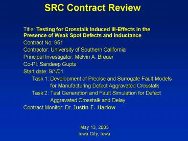
Title: SRC Contract Review
1
SRC Contract Review
- Title Testing for Crosstalk Induced Ill-Effects
in the Presence of Weak Spot Defects and
Inductance - Contract No 951
- Contractor University of Southern California
- Principal Investigator Melvin A. Breuer
- Co-PI Sandeep Gupta
- Start date 9/1/01
- Task 1 Development of Precise and Surrogate
Fault Models - for Manufacturing Defect Aggravated
Crosstalk - Task 2 Test Generation and Fault Simulation for
Defect - Aggravated Crosstalk and Delay
- Contract Monitor Dr. Justin E. Harlow
- May 13, 2003
- Iowa City, Iowa
2
Contract No. 951Testing for Crosstalk Induced
Ill-Effects in the Presence of Weak Spot Defects
and Inductance
3
Task Description - Task 1 951.001
- Title Development of Precise and Surrogate Fault
Models for Manufacturing Defect Aggravated
Crosstalk - Description Develop suitable fault models for
comprehensive yet efficient test development
crosstalk in conjunction with process variations
and manufacturing defects.
gtgt
4
Anticipated Results - Task 1 951.001
- Identify the conditions for excitation and
propagation of effects of defects. - Classify the defects based on their
characteristics. Define each alternative precise
fault model as a defect type along with the
conditions for excitation and propagation. - Consider alternative types of targets to obtain
additional alternative precise fault models. - Consider simplified versions of the precise fault
models to obtain surrogate fault models.
Surrogate models will be based on (1) elimination
of some targets from a precise fault model, and
(2) simplification of the conditions of
excitation and propagation. - Use the test generation and fault simulation
frameworks described next to conduct experiments
to identify the fault models that capture each
type of defect at the least complexity.
5
Task Deliverables - Task1 (Contd)
- Annual review presentation (Q2 02)
- A report describing precise fault models
determined by inserting realistic defects into
layouts, for each type of defects (Q3 02)
Delete - A report comparing path oriented and node
oriented fault models as well as models obtained
for different defect types (Q4 02) Q3 03 - A report summarizing how classical delay fault
testing is inadequate for detecting some defects
that, along with crosstalk, produce an
unacceptable amount of delay (Q4 02) - A report describing alternative surrogate fault
models (Q1 03)
Bold face - done Rescheduled not in
original proposal
6
Task Deliverables - Task1 (Contd)
- Annual review presentation (Q2 03)
- A report providing detailed comparison of
alternative fault models, precise and surrogate
(Q1 04) - Annual review presentation (Q2 04)
- A report detailing the revisions to the fault
models and detailing the recommended fault models
based upon employing the researchers test
generation and fault simulation framework (Q3
04) - Final report summarizing research accomplishments
and future direction (Q3 04)
Bold face - done Rescheduled not in
original proposal
7
Task Description - Task 2 951.002
- Title Test Generation and Fault Simulation for
Defect Aggravated Crosstalk and Delay - Description Develop techniques and tools for
test generation and fault simulation of crosstalk
in conjunction with process variations and
manufacturing defects. The tools developed are
expected to replace classical tools for delay
test development and timing analysis.
gtgt
8
Anticipated Results - Task 2 951.002
- Develop a general framework for test generation
that encompasses fault models identified in Task
1. This framework will (1) work with an arbitrary
value system, (2) consider different types of
targets and conditions for their detection, (3)
embody a general approach to handle the effect of
defects on gate/line delays, and (4) search the
space of all possible vector pairs in alternative
ways. - Develop a framework for simulation for the
proposed fault models, considering estimation of
the accuracy with which effects of defects on
timing are captured, metrics for coverage, and
managing the complexity of fault simulation.
9
Anticipated Results - Task 2 (Contd)
- Customize these tools for each alternative fault
model (precise and surrogate) for run time and
test application complexity comparisons of fault
models. Perform approximate equivalence and
approximate dominance between faults. Make final
recommendations regarding suitable fault models.
- Customize the above test generation and fault
simulation frameworks to obtain efficient ATPG
and fault simulators for the recommended fault
models.
10
Task Deliverables - Task2
- Annual review presentation (Q2 02)
- A report describing our efficient static timing
analysis and incremental timing refinement for
considering cyclic timing dependency caused by
multiple crosstalk sites for either worst case
delay paths or entire circuit (Q2 02) - An efficient static timing analysis tool for
considering cyclic timing dependency caused by
multiple crosstalk sites for either worst case
delay paths or entire circuit (Q2 02) - A tool embodying and a report describing the
general timing-oriented ATPG framework for the
range of fault models developed in Task 1 (Q3
02) Q4 03
Bold face - done Rescheduled not in
original proposal
11
Task Deliverables Task2 (Contd)
- A new framework for dynamic timing analysis to
identify tight lower and upper bound on delays of
a logic block (Q4 02) Q2 03 - A report of a new framework for dynamic timing
analysis to identify tight lower and upper bounds
on delays of a logic block (Q4 02) Q2 03 - A framework for fault-free version of timing
oriented test generation (value assignment,
implication, justification, search scheme) (Q4
02) Q4 03 - A tool embodying and a report describing the
general fault simulation framework for the range
of fault models developed in Task 1 (Q4 02) Q4
03 - A report describing the customization of the
above tools to each fault model (Q2 03) Q1 04
Bold face - done Rescheduled not in
original proposal
12
Task Deliverables Task2 (Contd)
- Annual review presentation (Q2 03)
- A report describing the comparison of alternative
fault models and recommended fault models,
including any new fault models developed as a
result of the in-depth analysis conducted using
the framework of tools (Q4 03) - Annual review presentation (Q2 04)
- Tools embodying and a report describing efficient
ATPG and fault simulation tools for each
recommended fault model (Q3 04) - Final report summarizing research accomplishments
and future direction (Q3 04)
13
Technology Transfer Contract No. 951
14
Overviews
- Process flow
- Analyzing crosstalk in the presence of weak
bridge defects - Analytic models for weak spot defects and
crosstalk - Testing combination of crosstalk and delay
defects via surrogate fault models - A framework of dynamic timing analysis
15
Process Flow
Process Variation
Delay Model Crosstalk Model
Defects
All Targets
Parasitics
Target Identification
Fault Modeling
Estimation/ Extraction
Validation Static/Dynamic Timing
Analysis Multiple Crosstalks
ATPG Engine
Timing Simulation
Layout
Transistor/gate-level netlist
Fault Models
Design Errors
Timing Ranges (Static/Dynamic)
Fix?
Fault Simulation
Redesign
Yes
No
Test Generation Multi-Valued Algebra Propagation
Conditions Multiple clocks
ATPG Engine
Timing Simulation
Fault Coverage
Tests
16
Analyzing Crosstalk in the Presence of Weak
Bridge Defects
17
Outline
- Introduction
- The circuit configuration used in our simulation
study - Slow-down/Speed-up created by a bridge between
two long lines (Conclusions C1-C5) - Interaction of bridge with crosstalk coupling at
separate sites (Conclusion C6) - Bridge and crosstalk coupling at the same site
(Conclusions C7 and C8) - Summary and future work
18
Introduction
- Slow-down, speed-up and pulse caused due to
capacitive crosstalk have been previously
analyzed - A framework to generate tests for the above
crosstalk effects has been developed - No test generation framework exists that
considers combination of weak spot defects and
crosstalk - A large portion of common defects manifest as
bridges between or opens at circuit lines
Ferguson, Shen88, Jee, Ferguson93, Hawkins,
Soden, Righter, Ferguson94 - Our long term goal To characterize the effects
of combinations of weak spot defects and
capacitive crosstalk and to develop a framework
to generate tests that provide coverage of such
combinations.
19
The configuration used in our study
del_x
del_y
- Based on an existing SCMOS cell library from
MOSIS, implemented in TSMC 0.25µ, four inverter
cells are defined inv1, inv2, inv4 and inv8 - Two 1000µ interconnects are modeled using
10-stages - The configuration can be set up to represent a
bridge site, a crosstalk coupling site or a site
with both effects
20
Slow-down and Speed-up created by a bridge
between two long lines
- Effect of bridge position and resistance value
- The bridge may be placed between one of the 11
nodes in the upper line and one of those in the
lower line (121 cases)
Example case in_x rising transition, in_y
static 0, inv_x, inv_y, inv_u and inv_v are all
inv1
del_x
del_x
Bridge Resistance
Bridge Resistance
- C1 (Bridge position) The dependence of the delay
on the bridge position is significant only for
bridge values close to the Critical Resistance
- C2 (Critical Resistance of a bridge) The
Critical Resistance of a bridge depends on the
strengths of the drivers
21
Bridge between two long lines (Cont.)
- Effect of skew between input transitions
Example case in_x rising in_y falling
inv_xinv1 inv_yinv1 inv_uinv1 inv_vinv1
RBr 1KO
in_x (Volts)
Time (S)
out_u (Volts)
Time (S)
in_y (Volts)
Negative Skew Positive Skew Fault free case
Time (S)
out_v (Volts)
Time (S)
- Components of delay Changes in arrival and
transition times
22
Bridge between two long lines (Cont.)
- Effect of skew between input transitions
Example case in_x rising, in_y falling,
inverters are all inv1.
del_y
del_x
Skew(ps)
Skew(ps)
tra_v
tra_u
- C3 (Bridge delay variations at small skews) For
skew values close to zero, a small change in skew
at a bridge site can significantly change the
delay and the transition time
Skew(ps)
Skew(ps)
23
Bridge between two long lines (Cont.)
- Effect of skew between input transitions
Example case in_x rising, in_y rising,
inverters are all inv1.
del_y
del_x
Skew(ps)
Skew(ps)
- C3 (Bridge delay variations at small skews) For
skew values close to zero, a small change in skew
at a bridge site can significantly change the
delay and the transition time - For all the possible combinations of in_x and
in_y (rising/rising, rising/falling,
falling/falling, falling/rising), for one type
skew (positive or negative), we have slow-down
and for other type of skew we have speed-up
24
Bridge between two long lines (Cont.)
- Effect of driver strengths and load
- C4 (Bridge delay dependence on driver and load)
Weaker drivers and larger output loads increase
the severity of a bridge-induced slow-down
- Effect of input transition times
- C5 (Bridge delay dependence on input transition
time) Increase in input transition time
increases the severity of bridge-induced
slow-down but has negligible impact on
bridge-induced speed-up. Furthermore, change in
input transition time has little impact on
severity of slow-down at lines where the
bridge-induced slow-down is already large.
25
Interaction of a bridge with a crosstalk at a
separate site
- A bridge site followed by a separate crosstalk
site
- No bridge present
- Bridge exists
26
Bridge and crosstalk at separate sites (Cont.)
- A bridge site followed by a separate crosstalk
site
Bridge site inv_x and inv_y are inv1, inv_u
and inv_v are inv4, RBR10KO
Example
The slow-down caused by the bridge can be up to
115 ps.
115 ps
Coupling site inv_x and inv_u are inv4, inv_y
and inv_v are inv1, C150fF
del_y
570ps
Skew(ps)
- Extra crosstalk delay due to decrease in skew
- between the affecting and victim line 570ps
115ps
- Total slow-down 115ps 570ps 685ps
- If the bridge site is immediately followed by
the - crosstalk site, the increase in delay will be
even more
27
Bridge and crosstalk at separate sites (Cont.)
- A bridge site followed by a separate crosstalk
site
- C6 (Synergistic delay effects of bridge and
crosstalk at different sites) A weak bridge and
a capacitive crosstalk in its transitive fanout
may together create a total slow-down well in
excess of the sum of their individual slow-downs
- A bridge site in transitive fanout of a separate
crosstalk site
28
Bridge and coupling at the same site
Example case in_x rising, in_y falling,
inverters are all inv1. Coupling capacitance is
50fF which is realistic for two 1000µ
interconnects, one in metal1 and the other in
metal2.
Couplingbridge case modified-bridge-only case
del_y
Skew(ps)
RBRInfinite RBR10KO RBR3KO
29
Bridge and coupling at the same site (Cont.)
Example case inverters are all inv1, Coupling
cap50fF, RBR1KO
in_x (Volts)
Time (S)
in_y (Volts)
Time (S)
Initial value not equal to Vdd Final value not
equal to Vss
sub_x_5 (Volts) (Bridge node)
Couplingbridge case Coupling only case
Time (S)
out_u (Volts)
Time (S)
30
Bridge and coupling at the same site (Cont.)
- For opposite direction transitions at in_x and
in_y, initial value (final value) at the bridge
node is neither Vdd nor Vss
- C7 (Interaction between coupling and bridge at
the same site) For values of skew around zero,
the speed-up/slow-down created by a crosstalk
coupling and a weak bridge at the same site is
less severe than when only the crosstalk coupling
is present
31
Bridge and coupling at the same site (Cont.)
- Crosstalk test invalidation due to weak bridge
defects
Example case in_x rising, in_y falling,
inverters are all inv1, Coupling cap50fF
5.60 E-10
RBRInfinite RBR10KO
4.50 E-10
del_y
- Example situation
- Assume that the delay of 560ps can cause an
observable error
170
-70
100
Skew(ps)
- Assume a test generator is available which
only considers coupling effect - Assume the test found invokes rising and
falling at the site with skew of 100ps, a
legitimiate test according to the curve for
RBrinfinite
- If RBr10kO, the real delay will be 450ps
- If the test generator had found another test
invoking a skew in the range of (510ps) to
(70ps), the error would have been observed
32
Bridge and coupling at the same site (Cont.)
- Crosstalk test invalidation due to weak bridge
defects
- C8 (Crosstalk test invalidation due to a weak
bridge at the same site) A crosstalk test may be
invalidated due to the presence of a weak bridge
at the crosstalk site
33
Summary
- An extensive simulation study of various
combinations of resistive bridges and crosstalk
has been performed - Several notable properties that have significant
implications for test development have been
discovered and highlighted, the most important of
which are - The slow-down caused due to a bridge is very
sensitive to the value of skew for skew values
close to zero (conclusion C3) - A combination of a bridge at one site and a
crosstalk at a separate site in its transitive
fanout (or vice versa) can cause slow-down whose
magnitude significantly exceeds the sum of the
slow-downs caused by each effect in isolation
(conclusion C6). - A test vector generated for crosstalk may in fact
be invalidated due to the presence of a weak
bridge at the crosstalk site (conclusion C8).
34
Future work
- The above study exposes several issues of
significant interest in test development and
provides the motivation for a more analytical
study, the objectives of which are - To amplify and analyze the results presented
above, by identifying root-causes and
analytically capturing the trends. - To study the type of combinations of defects and
crosstalk that will not be identified by static,
delay, and even crosstalk tests and hence must be
targeted using a framework that considers
combinations of crosstalk and weak spot defects
35
Analytic model and analysis for resistive bridge
in the presence of crosstalk
36
Outline
- Introduction
- Modeling
- Analytic derivations and equations
- Analysis for pulse and delay
- Summary
37
Introduction
- Previous models
- Crosstalk models
- Only considered crosstalk effects
- Resistive bridge fault model
- Only considered resistive bridge
- Treated skew of inputs as either 0 or a large
value - New analytic model
- Considers bridge with crosstalk effects
- Handles skew value as a variable
Z. Li, X. Lu, W.Q. Qiu, W.P. Shi, D.M.H. Walker,
A circuit Level Fault Model for Resistive Opens
and Bridges, Proc. VTS., pp.379-384, 2003.
38
Circuit with bridge and crosstalk
Circuit with coupling capacitance only
Circuit with bridge and coupling capacitance
In above circuits, A/V -- Far end point at
Affecting/Victim line
39
Driver modeling
- Represent driver as input voltage source and
equivalent resistance.
Reff Equivalent resistance Tr,Tf
Transition time of inputs Ar,Af Arrival time
of inputs Af Ar delta Tf,Tf Transition
time of outputs Af,Af Arrival time of
outputs
Real circuit with inverter
Equivalent circuit
Compute Af, Tf and Reff such that Af Af and
Tf Tf.
40
Lumped model
A/V --- node or signal on the
Affecting/Victim line Ca/Cv --- line
capacitance and gate capacitance of the
load Ra/Rv --- line resistance and drivers
equivalent resistance Cm --- coupling
capacitance Rb --- bridge resistance
41
General analytic model
Equivalent s-domain circuit
Time domain circuit
Ain/Vin --- input signal of driver Ainit/Vinit
--- initial voltage on node A/V when time t0-
42
Normalizing VDD to 1 and GND to 0, we obtain
,
,
where u and w are roots of the quadratic in s
,
u and w are negative.
.
- Interpret above equations as
- Signal A (response due to Ain)
(coupling from line V due to Vin)
(response due to Ainit and Vinit) - Signal V (response due to Vin)
(coupling from line A due to Ain)
(response due to Ainit and Vinit)
43
- Bridge and crosstalk induced pulse analysis
Initial voltages at node A and node V are 0.
Assume Ain(t) e-xt, where 1/x is the time
constant.
44
Time domain expression of victim line
,
- where . (u, w and Cr are
previously defined.) - V(t) is the sum of signals coupled from affecting
line - - through bridge
- - through coupling capacitance
- Further analysis
45
- Bridge critical resistance
- Critical resistance Maximum bridge resistance
for which a steady state logic error can
occur at outputs of receivers - Critical resistance max (
, ) - A threshold/V threshold Threshold voltage of
Affecting/Victim line receiver
46
- Bridge critical resistance
- Critical resistance Maximum bridge resistance
for which a steady state logic error can
occur at outputs of receivers - Critical resistance max (
, ) - A threshold / V threshold Threshold voltage of
Affecting/Victim line receiver
critical resistance gt
0 -gt 1
Vdd Vthreshold Gnd
47
- Dependence on the bridge resistance
- ? difference between amplitude and steady
state voltage on the victim line. - ? is proportional to bridge resistance.
- Dependence on the size of drivers
- Pulse amplitude is directly proportional to
driver size of the affecting line. - Pulse amplitude is inversely proportional to the
driver size of the victim line.
Results correlate with HSPICE for pulse analysis
48
Bridge and crosstalk induced delay analysis
Initial voltages at t0- of node A and node V
are 1/x and 1/y are time constants for Ain and
Vin, respectively.
49
- Transition at Vin arrives first (skew zgt0)
- Ain(t)e -x(t-z) and Vin(t)1-e -yt
- Transition at Ain arrives first (skew zlt0)
- Ain(t)e x t and Vin(t)1-e y (t-z)
Ap14,An14,Vp14 and Vn14 are constants. ? is
the step function.
50
- Observations
- is steady state voltage of A.
- is steady state voltage of V.
By decomposing V(t) into three components
-- (response due to Vin) (coupling from line A
due to Ain) and (response due to Ainit and
Vinit), show the dependences of components on
bridge resistance.
Results correlate with HSPICE.
51
- Delay variations at small skews
- Considering delay from 0.5Vdd Vin to 0.5Vdd V,
- a small change in skew can change the delay
significantly when skew value is close to 0.
52
- Bridge delay dependence on skew
- When skew is positive, speedup occurs at victim
line. - When skew is negative, slowdown occurs at victim
line.
gtgt
53
- Signal V (response due to Vin)
(coupling from line A due to Ain)
(response due to Ainit and Vinit).
54
and response due to Ainit and Vinit
remain relatively constant with respect to input.
55
- Coupling from line A due to Ain causes speedup.
56
Summary
- Analytic model combining bridge and crosstalk
effects. - Equations derived and shown to match HSPICE
simulations.
Jump to next section
57
BACKUP FIGURES
58
Equivalent resistance and input transition time
- All the experiments performed are using TSMC 0.25
technology. If not specially stated, the length
of the transistor is 2?. For unit sized inverter,
the width of PMOS is 26 ? and of NMOS is 7 ?. - For unit sized inverter,
- Reff 1.7k.
- Equivalent transition time TrTr0.35656ps,
where Tr is the input transition time of the
inverter circuit. - For inverter whose size is 2,
- Reff 0.9k.
- Equivalent transition time TrTr0.32462ps.
Back
59
Error on the output transition time.
For unit sized inverter
Next table
60
For inverter of size2
- Error on the output transition time is below
10. - Further improve the accuracy by considering the
transition time as a function of load capacitance
and line resistance.
back
61
Estimating delta
Delta vs. line resistance. The curves from top
to bottom are obtained for the input transition
time varying from 0.6ns to 0.1ns.
Next Page
62
Dependences of delta on the load capacitance and
input transition time.
back
63
u and w vs. bridge resistance. Plotted for a
normal circuit configurations
back
64
V(t) and its component signals when bridge
resistance is 1k ohm
Vb(t) signal coupled thru bridge Vc(t) --
signal coupled thru coupling capacitance
Next page
65
V(t) and its component signals when bridge
resistance is 10k ohm
Next page
66
V(t) and its component signals when bridge
resistance is 100k ohm
Signal coupled thru bridge determines the
steady state voltage. Signal coupled thru
coupling capacitance determines the pulse
amplitude.
back
67
Pulse analysis
Computed waveform
HSPICE simulation
Note We havent shifted the input by delta. So
there is a delay difference.
back
68
Component signal dependences on bridge resistance
- For coupling from line A due to Ain
- Amplitude is inversely proportional to bridge
resistance. - Decays faster as bridge resistance increases.
Kvn1(t,100000) stands for the component signal
when bridge is 100k Ohm. Vdd / Gnd are normalized
to 1 / 0.
Next Page
69
- For response of Vin ,
- Amplitude is proportional to the bridge
resistance.
Next Page
70
- For response due to the initial voltages,
- Amplitude is inversely proportional to bridge
resistance.
The negative pulse of 100k curve shows coupling
capacitance draw current from victim line when
affecting line falls.
Next Page
71
- Signals with different skew values
- Vin arrives first (Skew 0.1ns)
Victim line
Affecting line
A(t,100000) means the signal at node A when
bridge resistance is 100k. V(t,100000) means the
signal at node V when bridge resistance is
100k. Vertical axis ---voltage. Horizontal
axis ---time in units of second.
Next Page
72
Ain arrives first (Skew -0.1ns)
Victim line
Affecting line
back
73
Delay of victim line HSPICE result vs. analytic
result
Analytic result
HSPICE
back
74
Testing Combination of Crosstalk and Delay
Defects via Surrogate Fault Models
75
Outline
- Introduction
- Problem definition
- Robust path delay testing and its applicability
to our framework - Timing-independent testing of crosstalk targets
- Proposed surrogate targets for timing-independent
testing of a crosstalk target - Future and ongoing work
76
Introduction
- A capacitive coupling between an affecting and a
victim line with transitions in opposite
directions results in a slow-down at the victim
line - Severity of the slow-down effect depends on the
skew between the transitions - The slowed-down transition is propagated along
some paths to circuit outputs - Delay of the propagated transition depends on
- Arrival time of the transition at the victim line
and - Delay of the propagation paths from the victim
line to the outputs - Timing-oriented Test Generator is required
- The timing-oriented test generation approaches
have been extended to take into account
variations in delays due to variations in
manufacturing process
77
Problem Definition
- Each crosstalk target must be considered in the
presence of variations in manufacturing process
and delay defects of varying severities present
at arbitrary locations in the circuit - A timing-oriented test generator can not
guarantee the detection of the target in all
manufactured copies of the circuit
78
Problem Definition
- Our objective To develop a new approach to
generate tests for each crosstalk target in the
presence of manufacturing variations and delay
defects - Approach
- For a given crosstalk target, a set of surrogate
targets is identified - For each surrogate target, (necessary and)
sufficient conditions that a test must satisfy
for its detection are identified - The tests generated for the surrogate targets are
collectively guaranteed to detect the crosstalk
target in the presence of arbitrary delay defects
79
Robust path delay testing and its applicability
to our framework
- The path delay fault model, considers delay
defects of arbitrary multiplicity at arbitrary
locations and of arbitrary severities - Robust path delay testing provides a
timing-independent approach for generating tests.
The three key requirements are - A two-vector test for a target path delay fault
must propagate a transition via every on-path
gate (complete path transition requirement) - At each on-path gate, the values applied at the
off-path inputs must be such that the transition
at the output of the gate cannot occur unless the
transition at the on-path input of the gate has
propagated to its output (on-path transition
sequencing requirement) - Tests must be generated for all possible path
delay faults. The generated tests collectively
guarantee that the maximum delay is invoked for
the entire circuit
80
Robust path delay testing and its applicability
to our framework
- Complete path transition requirement captures the
cumulative effect of arbitrary numbers of delay
defects along the target path - On-path transition sequencing requirement ensures
that off-path defects can only slow-down the
transition being propagated along the target path - The above two conditions guarantee (under the
pin-to-pin delay model for each gate) that a
robust test for a target invokes the maximum
delay for the target path delay fault - The robust path delay test requirements can
capture the effects of arbitrary delay defects in
a timing independent manner - An attractive starting point for testing
crosstalk slowdown in the presence of multiple
delay defects
81
Timing-independent testing of crosstalk targets
- A crosstalk slow-down target (Affecting,
direction, Victim, direction) (x,R,y,F),
(x,F,y,R), (y,R,x,F), (y,F,x,R). - SP1, SP2, , SPn all possible n sub-paths that
end at x - SP?1, SP?2, , SP?m all possible m sub-paths that
end at y - SP??1, SP??2, , SP??p all possible p sub-paths
that start at y and end at a primary output
82
Timing-independent testing of crosstalk targets
- Let us focus on (x,R,y,F). A test for this target
must - (a) propagate a transition along a sub-path that
ends at the affecting line, say along SPi (1 i
n), to cause a rising transition at the x - (b) propagate a transition along a sub-path that
ends at the victim line, say along SP?j (1 j
m), to cause a falling transition at y - (c) propagate the slowed-down transition at y
along a sub-path that starts at y and ends at one
of the outputs, say along SP??k (1 k p) - Concatenation of SP?j and SP??k SP?j SP??k, a
path from an input to an output that passes via y
and causes a falling transition at y
83
Timing-independent testing of crosstalk targets
- The conditions (b) and (c) can both be satisfied
by propagating a transition along SP?j SP??k - By applying the complete path transition and
on-path transition sequencing requirements to
this path, the worst-case delay for this path is
invoked in a manner that the cumulative effects
of all delay defects along the path is captured
while the delay defects at other lines can only
add to this paths delay - By satisfying the complete (sub-)path transition
and on-(sub-)path transition sequencing
requirements along sub-path SPi the condition (a)
is also captured
84
Timing-independent testing of crosstalk targets
- How to take into account the key variable that
governs the quality of a test for a crosstalk
slowdown target namely the skew between the
arrival times at x and y? - This cannot be captured by directly applying the
complete (sub-)path transition and
on-(sub-)path transition sequencing requirements
to any combinations of the above (sub-)paths - The robust path delay testing requirements need
to be extended to capture all possible skew
values between affecting and victim lines
85
Timing-independent testing of crosstalk targets
- Proposed surrogate targets for timing-independent
testing of a crosstalk target
- A set of surrogate targets for the crosstalk
target must be presented - For (x, R, y, F), there are a total of n.m.p
surrogate targets written as triplets of
sub-paths, (SPi, SP?j, SP??k), where 1 i n,1
j m, 1 k p - Timing-independent requirements that a test for a
surrogate target must satisfy shall be presented - Collectively, any set of tests that satisfies
these requirements for all surrogate targets
corresponding to a given crosstalk target is
guaranteed to detect the original crosstalk target
86
Timing-independent testing of crosstalk targets
- Proposed surrogate targets for timing-independent
testing of a crosstalk target
- The (necessary and) sufficient timing-independent
conditions that we impose on a test for each
surrogate target - Lemma 1 (A test for a surrogate) A two-vector
sequence is said to be a test for a surrogate
target given by the triplet of sub-paths,
(SPi, SP?j, SP??k), if it - (a) r-robustly propagates a transition along
sub-path SPi to cause a rising transition at x - (b) r-robustly propagates a transition along
sub-path SP?j to cause a falling transition at y - (c) robustly propagates a transition along
sub-path SP??k - A two-vector sequence is said to r-robustly
propagate a transition along a sub-path if it
causes appropriate transitions at outputs of
on-path gates while implying steady
non-controlling values at off-path inputs of
on-path gates
87
Timing-independent testing of crosstalk targets
- Proposed surrogate targets for timing-independent
testing of a crosstalk target
- Theorem 1 (Timing independent testing of a
crosstalk slowdown target) A set of two-vector
sequences comprised of one test for each
surrogate target corresponding to a given
crosstalk slowdown target is guaranteed to detect
the given crosstalk slowdown target even if an
arbitrary number of delay defects are present in
the circuit under test - The proof of the above theorem is based on the
fact that any set of tests for the surrogate
targets (as defined in Lemma 1), ensures that all
possible values of skew between the transitions
at affecting and victim line are invoked, even in
the presence of arbitrary (multiple) delay
defects. When combined with the fact that these
tests (collectively) robustly propagate
transitions along every path passing via the
victim line, this establishes the completeness of
the proposed set of tests
88
Future and ongoing work
- Investigating the complexity of test generation
and size of test sets generated under this
approach - Investigating cases where the type of tests
defined in Lemma 1 do not exist for some (or
many) of the surrogate targets associated with a
crosstalk slowdown target - -To deal with such cases, less restricted
versions of the proposed tests (similar to
non-robust and other less restrictive tests for
path delay testing) will be developed that can be
used if some timing assumptions can be made or
verified - Investigating how the above conditions can be
simplified in scenarios where the type of delay
defects can be restricted. In particular, cases
are being considered where only significant
process variation or a single delay defect can be
assumed to exist
89
Dynamic Timing Analysis
4/2/2003 v2.1
90
DTA in Block Diagram
Value system
Crosstalk model
Timing analysis with crosstalk
Test generator for crosstalk
Timing analysis for partially specified vectors
Filtering
Delay model
Crosstalk targets
91
Dynamic Timing Analysis (DTA)Previous Results
- Integrated timing models
- More accurate gate delay and crosstalk models are
integrated to handle ranges of timing information
(13 compared to HSPICE) - Hazards are ignored
- An efficient methodology is developed to perform
timing analysis with multiple crosstalk effects - At top level, circuit viewed as a combination of
TISs (timing iterative sub-circuits) and gates - Only one iteration is needed for timing analysis
at the top level of abstraction - Multiple iterations may be required within each
TIS
92
Dynamic Timing Analysis (DTA)STA Vs. DTA
- STA (static timing analysis) Timing analysis for
fully unspecified vectors - DTA (dynamic timing analysis) Timing analysis
for partially or fully specified vectors
93
Dynamic Timing Analysis (DTA)Demonstration
Motivation
- 28 coupling capacitances are distributed in C880,
and the coupling capacitances vary from 16.1fF to
6.1fF - The gap between the maximum arrival time of
Static Timing Analysis (STA) 12.89 ns and 565000
random pattern simulations 11.4 ns is large and
indicates that a loose bound is obtained when
crosstalk is considered.
94
Dynamic Timing Analysis (DTA)Objectives
- To obtain tighter upper and lower bounds on
maximum circuit delay via DTA in presence of
single/multiple crosstalk (crosstalk sites may
cause cyclic timing dependencies)
95
Dynamic Timing Analysis (DTA)Types of Vectors
- Three types of vector pairs
- PVAT Partially-specified vector pair and actual
transition at PO (i.e. at least one vector-pair
in such space will have an actual transition) - FVAT Fully-specified vector pair and actual
transition at PO - PVPT Partially-specified vector pair and
potential transition at PO
96
Dynamic Timing Analysis (DTA)Improving Bounds
STA DTA
xx
4
10
PI1
Initial maximum delay for rising (4, 10)
xx
Circuit
PO1
PI2
xx
PI3
Only rising transition is demonstrated in the
example.
97
Dynamic Timing Analysis (DTA)Improving the Lower
Bound
- Helps tighten bounds on worst case delay
- Vectors need not cover the whole space for the
following two types of vectors - PVAT new_lower_bound Max(A_min)
- FVAT new_lower_bound Max(A_max)
- For the following case, PVPTs must span the
space - PVPT new_lower_bound Min(A_min)
Where A_min and A_max are the minimum and
maximum arrival times, respectively
98
Dynamic Timing Analysis (DTA)Improving the Upper
Bound
- Tighter upper bound can enable use of desired
clock period - Helps obtain tighter bounds on the maximum
circuit delay - In each case, vectors need to span the space of
all vectors - PVAT new_upper_bound Max(A_max)
- FVAT new_upper_bound Max(A_max)
- PVPT new_upper_bound Max(A_max)
99
Dynamic Timing Analysis (DTA)Selection of
Primary Input (SPI)
- PIs are prioritized based on the numbers of nodes
and crosstalk sites in each fan-out cone - The whole space is enumerated with either 00, 01,
10, or 11 at each input (4k combinations required
for k PIs) - Maximum of all A_max at POs used for the branch
and bound condition
100
Dynamic Timing Analysis (DTA)Experimental Results
101
Dynamic Timing Analysis (DTA)Experimental Results
- Unresolved space The maximum of A_max in this
subspace is still larger than the bound
102
Dynamic Timing Analysis (DTA)Experimental Results
- The percentage of unresolved space is lower when
the bound is larger.
103
Dynamic Timing Analysis (DTA)Required Time
- Required time The time interval during which the
desired transition should occur at a line for the
transition to propagate from the line to arrive
at a PO later than the sampling time.
gtgt
104
Dynamic Timing Analysis (DTA)Required Time
Computation without Crosstalk
- For every section of time stamps (TS)
- Forward timing implication is applied to check if
an overlap exists with the required time at the
output. If so, binary search is used to refine
the range within the TS. Otherwise, the next
section of TS is processed. - The union of the required time ranges are taken
from every branch for the required time of the
stem.
105
Dynamic Timing Analysis (DTA)Required Time
Computation without Crosstalk
- To-controlling transition
- The transition at any of the gates inputs should
not occur before R_mininput if the transition at
any input must be propagated to arrive at POs
later than a desired sampling time.
106
Dynamic Timing Analysis (DTA)Required Time
Computation without Crosstalk
- To-controlling transition
- For computing the output rise time for the
following gate, input fall times are considered.
107
Dynamic Timing Analysis (DTA)Required Time
Computation without Crosstalk
- To-controlling transition
- For computing the output rise time for the
following gate, input fall times are considered.
108
Dynamic Timing Analysis (DTA)Required Time
Computation without Crosstalk
- To-non-controlling transition
- The transition at an input must not occur before
R_mininput if it must be propagated to arrive at
POs after a desired sampling time.
109
Dynamic Timing Analysis (DTA)Required Time
Computation with Crosstalk
- Fix the arrival times to (TS1, TS2) at the inputs
of A, then apply the above procedure to obtain
the input required times for V.
110
Dynamic Timing Analysis (DTA)Empty Required Time
(ER)
- For the transition at one/more inputs of a gate
to propagate to POs so as to exceed the desired
sampling time. - Empty required time (ER)
- To controlling transition Any line with ER
should not have the transition as it will create
the transition at PO before the desired sampling
time. At least one of other inputs without ER
must have the transition to make the transition
at PO exceed the desired sampling time. - To non-controlling transition At least one of
inputs without ER must have a transition at time
greater than corresponding R_min to make the
transition at PO exceed the desired sampling
time. - Functional propagation conditions must be
satisfied at all gates along the path.
111
Dynamic Timing Analysis (DTA)Logic Condition
- For a specified path
- Logic conditions for side inputs
- For to-non-controlling transition at the gate
input, other gate inputs (side inputs) should
have (X, NC). - For to-controlling transition at the gate input,
other gate inputs (side inputs) should have (NC,
NC) and (NC, X) if the required time is ER and
non-ER, respectively.
X1/X1
11/1X
112
Dynamic Timing Analysis (DTA)Test for a Path
- For a delay of a target path to exceed the
sampling time at PO, a vector-pair may be found
if - Every line along this path is non-ER, i.e., it
must satisfy the required time condition. - All side inputs must satisfy the propagation
condition as well as required logic condition if
they have ERs.
113
Dynamic Timing Analysis (DTA)Branching and
Bounding Conditions
- Branching As long as there exists at least one
path whose delay is larger than the sampling time
at PO in the circuit, we assign a value at a PI
to enable appropriate transitions at one or more
lines along this path. - Bounding If this worst case delay at PO becomes
less than the sampling time, we backtrack
114
Dynamic Timing Analysis (DTA)Improved Selection
of Primary Input (ISPI)
- Perform required time computation for the circuit
- ER/non-ER
- Identify paths that can cause transition past the
sampling time at POs - For each path, assign desired transitions along
the path as well as necessary logic conditions at
side-inputs then perform backward implications - Combine the necessary condition cubes using the
union operation - Order PIs and enumerate all possible combinations
of values
115
Dynamic Timing Analysis (DTA)Union of Condition
Cubes
Circuit
PI1
1x
PO1
PI2
01
PI3
11
path
Circuit
PI1
10
PO1
PI2
x1
PI3
11
path
116
Dynamic Timing Analysis (DTA)Experimental Results
- The number of paths in C880 whose delay may
exceed the desired sampling time for STA and DTA
for different sampling times (ST).
117
Dynamic Timing Analysis (DTA)Experimental Results
118
Dynamic Timing Analysis (DTA)Experimental Results
- For the bound 12.45 ns, only 2 out of 49
sub-spaces remain after 9 PIs are enumerated
119
Dynamic Timing Analysis (DTA)Conclusions and
Ongoing Works
- Tighten the upper bound on maximum circuit delay
efficiently - Perform required time computation for the circuit
with crosstalk effects - Identify paths that can cause transition past the
sampling time at POs to help the order selection
of PIs - ER logic conditions used to assign necessary
conditions at side inputs - Tighten the lower bound on maximum circuit delay
efficiently - Apply random pattern simulation within good
quality sub-spaces - Apply DFS/ATPG
120
List of Papers
- Breuer, M. A., Gupta, S.K. (1996). Process
Aggravated Noise (PAN) New validation and test
problems, Proc. Int'l Test Conf., pp. 914-923,
Oct. 1996. - Breuer, M. A., Gupta, S.K. (2000). New Validation
and Test Problems for High Performance Deep
Sub-micron VLSI Circuits, Int'l Conf. on VLSI
Design, pp. 8, Jan. 2000. - Chen, L.C., Gupta, S.K., Breuer, M. A. (2000a).
Incremental Timing Refinement Intuition and
Development, SRC TECHCON, Oct. 2000. - Chen, L.C., Gupta, S.K., Breuer, M. A. (2000b). A
new framework for static timing analysis,
incremental timing analysis, and timing
simulation, Proc. of Asian Test Symposium, pp
102-107, Dec. 2000. - Chen, L.C., Gupta, S., Breuer, M. A. (2001a). A
new gate delay model for simultaneous switching
and its applications, Proc. of Design Automation
Conf., pp. 289-294, Jun. 2001. - Chen, L.C., Mak, T. M., Breuer, M. A., Gupta, S.
K. (2001b). Crosstalk test generation for pseudo
Intel circuits A case study, Proc. of Intl Test
Conf., pp. 548 -557, Oct. 2001.
121
List of Papers (Contd)
- Chen, L.C., Gupta, S., Breuer, M. A. (2002).
TA-PSV - Timing Analysis for Partially Specified
Vectors, Journal of Electronic Testing, vol. 18,
no. 1, pp. 73-88, Feb. 2002. - Chen, L.C., Gupta, S., Breuer, M. A. (2003).
Beyond Pin-to-Pin Delay Model, submitted to Proc.
of Int'l. Conf. on Computer-Aided Design, Oct.
2003. - Chen, W.Y., Breuer, M. A., Gupta, S.K. (1997).
Analytic model for crosstalk delay and pulse
analysis for non-ideal inputs, Proc. Int'l Test
Conf., pp. 809-818, Nov. 1997. - Chen, W. Y., Gupta, S. K., Breuer, M. A. (1998).
Test generation in VLSI circuits for crosstalk
noise, Proc. of Int'l. Test Conf., pp. 641-650,
Oct. 1998. - Chen, W. Y., Gupta, S. K., Breuer, M. A. (1999).
Test generation for crosstalk-induced delay in
integrated circuits, Proc. of Int'l. Test Conf.,
pp 191-200, Sept. 1999. - Chen, W. Y., Gupta, S. K., Breuer, M. A. (2000).
Test generation for crosstalk-induced faults
Framework and computational results, Proc. of
Asian Test Symposium, pp 305-310, Dec. 2000.
122
List of Papers (Contd)
- Chen, W. Y., Gupta, S. K., Breuer, M. A. (2002a).
Test generation for crosstalk-induced faults
Framework and computational results, Journal of
Electronic Testing, vol. 18, no. 1, pp. 17-28,
Feb. 2002. - Chen, W. Y., Gupta, S. K., Breuer, M. A. (2002b).
Analytical models for crosstalk excitation and
propagation in VLSI circuits, IEEE Trans. on
Computer-Aided Design of Integrated Circuits and
Systems, vol. 21, no. 10, pp. 1117 1131, Oct
2002. - Irajpour, S., Nazarian, S., Wang, L., Gupta, S.
K., Breuer, M. A.. (2003). Analyzing Crosstalk in
the Presence of Weak Bridge Defects, VTS 2003. - Natarajan, S., Gupta, S. K., Breuer, M. A.
(1998). Process variations and their impact on
circuit operation, Proc. of Int'l Symp. on Defect
and Fault Tolerance in VLSI Systems, pp. 73-81,
1998. - Natarajan, S., Gupta, S. K., Breuer, M. A.
(2001). Switch-level delay test of domino logic
circuits, Proc. of Int'l. Test Conf., pp.
367-376, Oct. 2001. - Huang, I. D., Gupta, S.K., Breuer, M.A. (2002).
Accurate and efficient static timing analysis
with crosstalk, Proc. of Int'l. Conf. on Computer
Design, pp. 265 -272, 2002.
123
List of Papers (Contd)
- Nazarian, S., Huang, H., Natarajan, S., Gupta, S.
K., Breuer, M. A.. (2002). XIDEN Crosstalk
target identification framework, Proc. of Int'l.
Test Conf., pp. 265-272, Oct. 2002. - Nazarian, S., Gupta, S. K., Breuer, M. A..
(2003). Efficient Filtering of Crosstalk Slowdown
Targets, will submit to Proc. of Asian Test
Symposium, Dec. 2003. - Sinha, A., Gupta, S. K., Breuer, M.A. (1999).
Validation and test generation for oscillatory
noise in VLSI interconnects, Proc. of Int'l.
Conf. on Computer-Aided Design, pp. 289-296, Oct.
1999. - Sinha, A., Gupta, S. K., Breuer, M.A. (2000).
Validation and Test Generation for Crosstalk
Noise on Multi-Point Nets , SRC TECHCON, Oct.
2000. - Sinha, A., Gupta, S. K., Breuer, M.A. (2001).
Validation and test generation for inductance
induced noise on VLSI interconnects, Proc. of
IEEE Workshop on Signal Propagation of
Interconnects, 2001. - Sinha, A., Gupta, S. K., Breuer, M.A. (2002).
Validation and test issues related to noise
induced by parasitic inductances of VLSI
interconnects, IEEE Trans. on , Advanced
Packaging, vol. 25, no. 3, pp. 329 339, Aug 2002
Recommended
