
FPX Overview for January 2001 Workshop - PowerPoint PPT Presentation
1 / 54
Title:
FPX Overview for January 2001 Workshop
Description:
Integrating FPGAs into an Internet Router. FPX Modules distributed across ... for fast table-lookups ... Hex.txt: HEX/ASCII Table. fake_NID_in.vhd: Utilities ... – PowerPoint PPT presentation
Number of Views:31
Avg rating:3.0/5.0
Title: FPX Overview for January 2001 Workshop
1
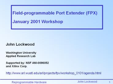
Field-programmable Port Extender (FPX)January
2001 Workshop
John Lockwood Washington University Applied
Research Lab Supported by NSF ANI-0096052 and
Xilinx Corp. http//www.arl.wustl.edu/arl/project
s/fpx/workshop_0101/agenda.html
2
Technologies for Implementing Networks
- Microprocessors
- Fully Reprogrammable
- Silicon resources dictated by CPU Vendor
- Mostly Sequential Processing
- Custom Hardware
- Highly concurrent processing
- Silicon resources optimized for application
- Static Functionality
- Reprogrammable Hardware
- Highly concurrent processing
- Silicon resources optimized for application
- Fully Preprogrammable
3
Integrating FPGAs into an Internet Router
IP Packets
IP Packets
- FPX Modules distributed across each port of a
switch - IP packets (over ATM) enter and depart line card
- Packet fragments processed by modules
4
Hardware Device
5
(No Transcript)
6
Architecture of the FPX
- RAD
- Large Xilinx FPGA
- Attaches to SRAM and SDRAM
- Reprogrammable over network
- Provides two user-defined Module Interfaces
- NID
- Provides Utopia Interfaces between switch line
card - Forwards cells to RAD
- Programs RAD
7
Infrastructure Services
8
Routing Traffic Flows Between Modules
- Traffic flows routed among
- Switch
- Line Card
- RAD.Switch
- RAD.Linecard
NID
- Functions
- Check packets for errors
- Process commands
- Control, status, reprogramming
- Implement per-flow forwarding
9
Typical Flow Configurations
10
Reprogramming Logic
- NID programs at boot from EPROM
- Switch Controller writes RAD configuration memory
to NID
- Bitfile for RAD arrives transmitted over network
via control cells
- Switch Controller issues Full/Partial
reconfigure command
- NID reads RAD config memory to program RAD
- Performs complete or partial reprogramming of RAD
11
Software Services for Controlling the FPX
- Methods of Communication
- - Fpx_control
- - Telnet
- - Web Interface / CGI
- - Basic_send
- - User Applications
- Software Plug-ins
- - Concepts
- - Functionality
- Emulation
- Nid_listener
- Rad_listener
Fip Memory
Manager
Remote
Applications
Read
WEB
Basic
Telnet
Fip
Access
Send
CGI
Basic
Send
Software
Controller
fpx_control
fpx_control
0.0
7.1
VCI 76 (NID), VCI 100 (RAD)
VCI 115 (NID), VCI 123 (RAD)
OC-3 Link
(up to 32 VCIs)
Washington University
NID
NID
Gigabit Switch
RAD
RAD
12
Pictorial view of fpx_control interfaced with
hardware
Fpx_control 0-7.0/1
13
Combination Router Hardware and Software
- Implement link speed opertions on hardware
- Implement higher-level functions in software
- Migrate functionality on the critical path
14
(No Transcript)
15
FPX Hardware
16
(No Transcript)
17
FPX SRAM
- Provide low latency for fast table-lookups
- Zero Bus Turnaround (ZBT) allows back-to-back
read / write operations every 10ns - Dual, Independent Memories
- 36-bit wide bus
18
FPX SDRAM
- Dual, independent SDRAM memories
- 64-bit wide, 100 MHz
- 64MByte / Module 128 Mbyte total expandable
- Burst-based transactions 1-8 word transfers
- Latency of 14 cycles to Read/Write 8-word burst
19
Hardware Device
20
Development of FPX Applications
21
FPX Interfaces Provides
- Well defined Interface
- Utopia-like 32-bit fast data interface
- Flow control allows back-pressure
- Flow Routing
- Arbitrary permutations of packet flows through
ports - Dynamically Reprogrammable
- Other modules continue to operate even while new
module is being reprogrammed - Memory Access
- Shared access to SRAM and SDRAM
- Request/Grant protocol
22
Network Module Interface
D_MOD_IN310
D_MOD_OUT310
Data Interface
SOC_MOD_OUT
SOC_MOD_IN
TCA_MOD_IN
TCA_MOD_OUT
Module Logic
SRAM_GR
SRAM Interface
SRAM_D_OUT350
SRAM_D_IN350
SRAM_ADDR170
SRAM_RW
SDRAM_REQ
SDRAM_GR
SDRAM_DATA630
SDRAM_DATA630
SDRAM Interface
SRAM_ADDR170
SRAM_RW
CLK
Module Interface
RESET_L
ENABLE_L
READY_L
23
Reprogrammable Application Device (RAD)
- Spatial Re-use of FPGA Resources
- Modules implemented using FPGA logic
- Module logic can be individually reprogrammed
- Shared Access to off-chip resources
- Memory Interfaces to SRAM and SDRAM
- Common Datapath to send and receive data
24
Combining Modules within the Chip
- Modules fit together at static I/O interfaces
- Partial reprogramming of FPGA used to
install/remove modules - Modules added and removed while other modules
process packts - Statically-configured Long Lines provide
chip-wide routing
Intrachip Module Switching
Data
SRAM
SRAM
SRAM
...
SDRAM
SDRAM
FPGAs Long Lines
Module Loading / Unloading
25
SDRAM Controller Interface
- Implements Burst Read/Writes to SDRAM
- Provides refresh signals to SDRAM
- Asserts RAS / CAS signals for address
- Provides standard Interface to Application
26
On-Chip sharing of SDRAM
- Implements on-chip and off-chip tri-state buses
- Shared wire resources used on-chip
- Arbitrates among multiple modules
- Allows multiple modules to share 1 SDRAM
27
Applications for the FPX
28
Pattern Matching
- Use Hardware to detect a pattern in data
- Modify packet based on match
- Pipeline operation to maximize throughput
29
Hello, World Module Function
30
Logical Implementation
Append WORLD to payload
VCI Match
New Cell
31
Source Concurrent VHDL Statements
- BData_Out_process process (clkin) begin
- -- buffer signal assignments
- if clkin'event and clkin '1' then
- d_sw_rad lt BData_Out -- (Data_Out
d_sw_rad) - BData_in lt d_sw_nid -- (Data_In
d_sw_nid) - BSOC_In lt soc_sw_nid -- (SOC_In
soc_sw_nid) - BSOC_Out lt BSOC_In
- BTCA_In lt tcaff_sw_nid -- (TCA_In
tcaff_sw_nid) - BTCA_Out lt BTCA_In
- ...
- counter lt nx_counter -- next state
assignments - ...
- state lt nx_state -- next state
assignments
32
Manifest of Files in HelloTestbench.tar
- File
- http//www.arl.wustl.edu/arl/projects/fpx/workshop
_0101/HelloTestbench.tar - Contains
- README.txt General Information
- Makefile Build and complile programs
- TESTCELL.DAT Cells written into simulation
(Hex) - CELLSOUT.DAT Data written out from simulation
- Hex.txt HEX/ASCII Table
- fake_NID_in.vhd Utilities to save cells to file
- fake_NID_out.vhd Utility to read cells from
file - top.vhd Top level design
- helloworld.vhd Top-level helloworld design
- pins.ucf Pin mapping for RAD FPGA
33
TestBench configuration
top
HelloWorld
NID_Out
NID_In
soc
34
Post-Synthesis Signal Timing
- Start_of_cell (SOC) Buffered across Edge flops
- data_in VCI5, PayloadHELLOEEO
- data_out HELLO WORLD.
35
Higher-Level Application Wrappers
36
The wrapper concept
37
AAL5 Encapsulation
- Payload is packed in cells
- Padding may be added
- 64 bit Trailer at end of cell
- Trailer contains CRC-32
- Last Cell indication bit (last bit of PTI field)
38
HelloBob module
HelloBob/MODULES/HelloBob/vhdl/module.vhdl
39
Applications IP Lookup Algorithm
40
Fast IP Lookup Algorithm
- Function
- Search for best matching prefix using Trie
algorithm - Contributors
- Will Eatherton, Zubin Dittia, Jon Turner, David
Taylor, David Wilke,
41
Hardware Implementation in the FPX
SRAM1
SRAM1 Interface
Remap VCIs for IP packets
Extract IP Headers
IP Lookup Engine
counter
On-Chip Cell Store
SRAM2
Control Cell Processor
Packet Reassembler
RAD FPGA
NID FPGA
SW
LC
42
Fast IP Lookup (FIPL) Application
Route add 141.142.5.0/24 8 Route delete
141.142.0.0/16
43
Conclusions
44
Conclusions (1)
- Reprogrammable Hardware
- Enables fine-grain, concurrent processing
- Provides Sea of functions
- Software upgradable
- Networking Module
- Contains a well-defined interface for
implementation of network function in hardware - Includes SRAM and SDRAM for table storage and
queuing
Data Interface
Module Logic
SRAM Interface
SDRAM Interface
Module Interface
45
Conclusions (2)
- Field Programmable Port Extender (FPX)
- Network-accessible Hardware
- Reprogrammable Application Device
- Module Deployment
- Modules implement fast processing on data flow
- Network allows Arbitrary Topologies of
distributed systems - Project Website
- http//www.arl.wustl.edu/arl/projects/fpx/
46
FPX Workshop Agenda Times and Location
- Thursday, Jan 11, 2001
- 8am Breakfast
- 5th floor Jolley Atrium
- 9am-Noon Session I
- Sever 201 Lab
- Lunch
- 5th floor Jolley Atrium
- 1pm-5pm Session II
- Sever 201 Lab
- Friday, Jan 12, 2001
- 8am Breakfast
- 5th floor Jolley Atrium
- 9am-Noon Session III
- Sever 201 Lab
- Lunch
- 5th floor Jolley Atrium
- 1pm-5pm Session IV
- Sever 201 Lab
On-line Agenda http//www.arl.wustl.edu/arl/proje
cts/fpx/workshop_0101/agenda.html
47
End of Presentation
48
Implementing DHP Modules in Virtex1000E
- Virtex 1000E logic resources
- Globally accessible IOBs
- 64 x 96 CLB array
- 4 flops/LUTs per CLB
- 96 Block SelectRAMs
- 4096 bits per block
- 6 columns of 16 blocks
- 6 columns of dedicated interconnect
- DHP Modules
- 64 x 12 CLB array
- (768 CLBs, 3072 flops)
- Double DHP Modules
- 64 x 24 CLB array
- (1536 CLBs, 6144 flops)
- 16 BRAMs (8KB) per Module
- 3 DHP Modules per path
- 1 SRAM interface per path
- 1 SDRAM interface per path
49
FPGA Design Flow
EDIF
VHDL
BIT
Download Xilinx bit
Spectrum
Xilinx Backend
VHDL Design
file to FPX FPGA
Timing
Logical Simulation
Verification
- Application groups develop RAD module
- Compile of Architecture
- Synthesize into LUT functions
- Route and place into CLB Array
- Verify timing of circuit to 100 MHz
50
Hello, World Silicon Layout View
51
Post-Synthesis Signal Timing
- Start_of_cell (SOC) Buffered across Edge flops
- data_in VCI5, PayloadHELLOEEO
- data_out HELLO WORLD.
52
Results Performance
- Operating Frequency 119 MHz.
- 8.4ns critical path
- Well within the 10ns period RAD's clock.
- Targeted to RADs V1000E-FG680-7
- Maximum packet processing rate
- 7.1 Million packets per second.
- (100 MHz)/(14 Clocks/Cell)
- Circuit handles back-to-back packets
- Slice utilization
- 0.4 (49/12,288 slices)
- Less than one half of one percent of chip
resources - Search technique can be adapted for other types
of data matching and modification - Regular expressions
- Parsing image content
53
Analysis of Pipelined FIPL Operations
Time (cycles)
- Throughput Optimized by interleaving memory
accesses - Operate 5 parallel lookups
- t_pipelined_lookup 550ns / 5 110 ns
- Throughput 9.1 Million packets / second
54
Hello, World Entity
RAD
NID
Recommended
CrystalGraphics Presentations


