
Tutorial on Electronic Transport PowerPoint PPT Presentation
1 / 61
Title: Tutorial on Electronic Transport
1
Tutorial onElectronic Transport
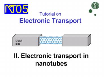
II. Electronic transport in nanotubes
2
Electrical measurements on individual tubes
- Nanotubes deposited or grown (CVD)
- Localize nanotubes (AFM)
- Electron-beam lithography to
- define electrodes
- Evaporate metal contacts on top
- (Au, Pd, Al, Ti, Co, )
200 nm
drain
source
- Nanotubes grown in house
- Electron-beam lithography to
- form electrodes
- Nanotubes are 1D metals and semiconductors
- Field effect transistors
- Quantum transport at low T
Au
SiO2
p Si gate
Vg
I
V
100 mm
3
Typical device fabrication
Electron beam lithopgraphy
Lift off
Another (UV) lithography step for bond pads
before mounting
4
AFM and alignment marks EFM
Technicality
Atomic Force Microscopy (AFM)
Electrostatic Force Microscopy (EFM)
EFM
AFM
SWNTs
12 mm
0.1 mm
Poster
Bockrath et al, NanoLetters (2002) Jespersen et
al, NanoLetters (2005)
T.S. Jespersen
5
Zoom in device
Poster
Henrik I. Jørgensen, NBI
6
Room temperature transport
drain
source
gate
Type II. Semiconducting tube
Type I. Metallic tube
ON
metal vs halvleder, gap between valence and cond
band of transistor, men ikke anvendelse som
hovedinteresse
(Naive sketch)
OFF
Band structure determined by the geometry
(chirality) of the molecule
Field-effect transistor
Wire
low T
Seen first by Tans et al, Nature (1998)
single electron effects
Data from Appl. Phys. A 69, 297 (1999).
7
Chirality determines bandstructure
although carbon atoms only!
Eg 0.5-1 eV
(N, M) (5, 5)
(N, M) (10, 5)
In reality, also Type III Small-gap
semiconducting tubes (zigzag metals)
8
Semiconducting nanotube FET
Performance of
First interpretation of
Field Effect Transistor
On
Linear increase in G-Vg ie limited by mobility
(diffusive transport) Slope dG/dVg
?Cg/L2 (from Drude ? ne?) ? ? ? 10,000
cm2/Vs (For silicon ? ? 450)
G (e2/h)
Off
Vg (V)
Off at positive Vg ? p type FET (Doped at
contacts and by adsorbed oxygen - sensor!)
Mobility ? vd / E electric field E
drift velocity vd
Saturation due to contact resistance, e2/h
- Off at positive Vg
- p type FET
- (intrinsic p doping?)
Later work showed importance of (Schottky)
contacts!
9
Schottky barriers in nanotube FETs
Band structure
Different workfunctions (eg due to O2 exposure)
Oxygen exposure
Schottky barrier
Vg-0.5 V
Vg0
Barriers thinnest for Vg lt 0, ie largest current
when p type
No change of gap
No shift of mid gap contacts (shape) modulated
Asymmetry due to modulation of contact Schottky
barriers
Heinze et al (IBM), PRL 89, 106801 (2002)
(Gas sensors)
10
Ballistic transport in metal tubes
4e2/h
1D conductor
- Near the theoretical limit 4e2/h (with two
subbands) - Close to Fermi level backscattering is
suppressed in armchair (metal) tubes by
symmetry
(Ballistic transport also possible in very short
semiconducting tubes, otherwise mostly diffusive)
Kong et al, PRL 87, 106801 (2001) McEuen et al,
PRL 83, 5098 (1999)
11
Quantized current limiting
Metallic tube with good contacts
I0 25 mA
Steady state current I0 4e/h Ephonon
4e/h 160 meV 15-30 mA
- High electric field transport
- electrons are accelerated
- emit (optical) phonons when EEphonon
- electron-phonon scattering for high bias
Z. Yao, C. Kane and C. Dekker PRL 84, 2941 (2000)
12
Metal contacts rarely ideal
Room temperature resistance of CVD grown SWNT
devices
Babic et al, AIP Conf. Proc. Vol. 723, 574-582
(2004) cond-mat
13
Room temperature transport
- Ballistic transport possible (near 4e2/h)
- - ideal wires
- - current limiting 25 mA
- Field effect transistors
- - high performance
- - optimised geometries (not shown)
- NB Nanotube quality and contact transparency are
important
14
Outline
- Electronic structure (1D, 0D)
- density of states
- Electron transport in 1D systems (general)
- quantization, barriers, temperature
- Transport in nanotubes (1D)
- contacts, field-effect,...
- Low temperature transport, quantum dots (0D)
- Coulomb blockade, shells, Kondo, ...
- Nanotube electronics, circuits, examples
- Problem session
- Wellcome party
15
Jia T-dep
Coulomb blockade oscillations in a metallic tube
device
Transport in metallic tube oscillations at low T
Seen first in data by Bockrath et al and Tans et
al (1997)
16
Power laws in tunneling
Typical T dependences
G T 0.6
BUT Similar power laws now found in multiwall
tubes experiments Bachtold et al, LANL
preprints ? Luttinger liquid isnt the whole
story! Theory Hakonen et al, Egger Gogolin,
LANL preprints
Bockrath et al, Nature (1999)
Evidence for Luttinger liquids Predicted Egger
Gogolin (1997), Kane, Balents Fischer (1997)
17
Initiator for breakthroughs 1997
Availability of high quality single walled
nanotube material (Smalley group, Rice
University, 1995-96)
Keep this in mind...
18
Low temperature transport
It is cryostat, it exists, OK, lets get on
20 mK
sample
Dilution refrigerator
19
Low temperature data
Gpeak 1/T
0.3 K 1.7 K 4.2 K
Coulomb blockade in the quantum regime below 4
K- Nanotube quantum dot
First by Tans et al. (1997), Bockrath et al.
(1997)
20
Coulomb blockade
BiasV
Electrons can tunnel only at Vg for which
E(N1,Vg) E(N,Vg) ? kT
Cost for adding one electron charging
energy EC Q2/C e2/C
21
Single-electron charging at low T
Add 1 e -
G (4e2/h)
Zero current !
1) large electrostatic charging energy U
e2/Ctotal 10 meV gt kBT 2) tunnel contacts
well-defined number N of electrons fixed
number N of electrons i.e. zero current !
except when E(N)E(N1)...
Gate voltage Vg (V)
Coulomb blockade
1) large electrostatic charging energy U
e2/Ctotal 10 meV gt kBT 2) tunnel contacts
well-defined number N of electrons fixed
number N of electrons i.e. zero current -
Coulomb blockade except when E(N)E(N1)...
RL
RR
N electrons
22
Published data not always typical...
T 4K
23
Non-linear characteristics
T 4.2 K
Nonlinear I-V curve (fixed gate volt.)
Coulomb blockade peaks (zero bias)
Differential conductance
Bias spectroscopy, Coulomb diamonds,
high
dI / dV
0
Appl. Phys. A 69, 297 (1999).
24
Ohmic resistor
Ohmic resistor
Color map of dI/dV
Bias voltage V
I
V
Gate voltage Vg
25
Interacting electrons at low T
Color map of dI/dV (white high R, blue low R)
Measurement at T 100 mK
Bias voltage V
Gate voltage Vg
inelastic process
level spacing (spectroscopy)
Coulomb blockade
many-body state (Kondo effect)
single electron tunneling
Electron transport governed by - tunneling
processes - discrete electron charge - orbitals
of the molecule - electron-electron
interactions and many-body effects
26
Transport spectroscopy of a tube quantum dot
27
Shell filling in closed dot
Constant Interaction model Addition energy eDVg
U DE
DVg
Molecular spectroscopy by electrical measurements
PRL 89, 46803 (2002)
28
4-electron shells and excited states
Experiment
Level structure
Model
5 parameters - charging energy U - level
spacing D - subband mismatch d lt D (small) -
exchange energy J (small) - residual Coulomb
energy dU
(Liang et al, PRL 88, 126801 (2002)) Sapmaz et
al, PRB 71, 153402 (2005)
29
Semiconducting quantum dotwith electron-hole
symmetry
Small-gap semiconducting tube (Type III., zigzag
metal)
First hole enters
First electron enters
Empty dot
Few-electrons dots can be made
Jarillo-Herrero et al, Nature 429, 389 (2005).
30
From closed to open quantum dots
G (T 300 K)
Tunnel contacts weak coupling limit
Coulomb blockade peaks
0.3 e2/h
G (e2/h)
1.7 e2/h
G (e2/h)
G (e2/h)
Metallic contacts - strong coupling limit
3.1 e2/h
Dips rather than peaks
31
Closed to open, II
Gray scale plots of the diffential conductance
dI/dV vs. Vg and V
1D quantum dot
Tunnel contacts weak coupling limit
V
V
V
Metallic contacts - strong coupling limit
1D molecular Fabry-Perot etalon Liang et al,
Nature (2001).
32
Fabry-Perot resonances in nanotube waveguide
- Generally high conductance a coherent electron
waveguide - Dips in conductance due to interference in the
resonant cavity
Liang et al, Nature 411, 665 (2001)
33
With medium-transparency contacts
M
dI/dV
X
Y
Y
75 mK
X
780 mK
- Alternations
- Peaks in dI/dV
- .G -logT
- Key signatures of the Kondo effect
Standard Coulomb Blockade
Nature 408, 342 (2000)
34
Cotunneling and Kondo
M
imagine
1.
2.
3.
EC
E0
Ground state
Virtual
Okay
Heisenberg Dt h/E0
Co-tunneling due to more open
contacts (higher order process)
35
The Kondo effect, correlations
So far just single-particle physics...
Anderson model
Normal ground state
For strong coupling (large V), new ground state
e2/C
Y
coherent superposition (when T low enough)
Coulomb blockade
predicts resonance for transport (for S1/2)
EXPERIMENT
Even Odd Even
2.0
75 mK
Odd N, S1/2 correlated state at really low
T, conductance restored!
Even N, S0 no correlated state, suppression of
conductance
shows to how great a detail we can harness
single charges and spin in these molecules
I (a.u.)
740 mK
Highly tuneable system
0.0
NB Nanotubes are ideal 1D metals
36
Supercond contacts
...recent data...
Warning Dirty experiments
37
Superconductor-SWCNT-Superconductor junction
Superconducting leads
Normal (B180mT), 30mK
Four-period shell filling. Ec ?E 3-4meV
Normal (B180mT)
SWCNT contacted to Ti/Al/Ti 5/40/5 nm leads (Tc
760mK)
Superconducting
Clear sign of Multiple Andreev Reflections, i.e.,
structure in dI/dV vs bias at Vn2?/en,
n1,2,3,...
-2?
2?
Poster
Kasper Grove-Rasmussen et al
38
Ferromagnetic contacts
39
Multiwall tubes with magnetic leads
K. Tsukagoshi, B.W. Alphenaar, H. Ago, Nature
401, 572 (1999)
Two-terminal resistance vs. B-field for three
different devices at 4.2 K
Diameter 30 nm
In the best case DR/Ra 9 Multiwall
tubes diffusive conductors intrinsic
magnetoresistance
SiO2
Si
40
Spin-polarized transport ?
Spintronics - single-electron spin
transistor? Probe spin-charge separation
T 4.2 K
Sweep directions
Current (nA)
Micromagnet electrodes, single-walled
Multidomain (MFM image)
External magnetic field (T)
The simplified picture
Anti-parallel
Jensen et al, PRB (June 2005)
Spin-tronics
Use the electronic spin rather than charge as
carrier of information
41
Gold nanoparticle single-electron transistor with
carbon nanotube leads
- CVD grown nanotubes (Cph)
- EBL (electron beam lithography) (Cph)
- AFM imaging and manipulation (Lund)
- low temperature transport measurements (Lund)
AFM manipulation
SiO2
Au
SiO2
What if the nanoparticle is (superpara-)magnetic?
(5-10 nm for Fe particles)
7 nm gold particle (e2/C60 meV)
C. Thelander et al, APL 79, 2106 (2001).
42
Electrons in nanotubes
Attach leads to 1D electron system Low T
measurements
Single-electron effects
Normal metal
- spectroscopy, shells (2, 4) - Fabry-Perot
resonances
Correlated states
Spin
- Kondo effect, long-range interactions,
- Luttinger liquid
Ferromagnet
Magnetic contacts
- Spin transport, spin transistors?
Superconductor
Superconducting contacts
- supercurrents?
Nanoparticle
AFM manipulation of nanoscale objects
- Gold particle transistor, 1D-0D-1D
43
Outline
- Electronic structure (1D, 0D)
- density of states
- Electron transport in 1D systems (general)
- quantization, barriers, temperature
- Transport in nanotubes (1D)
- contacts, field-effect,...
- Low temperature transport, quantum dots (0D)
- Coulomb blockade, shells, Kondo, ...
- Nanotube electronics, circuits, examples
- Problem session
- Wellcome party
44
Crossed Nanotube Devices
AFM image of one pair of crossed nanotubes
(green) with leads (yellow)
Optical micrograph showing five sets of leads to
crossed nanotube devices
Fuhrer et al., Science (2000)
45
Crossed Nanotube Junctions
- MM junctions
- R 100-300kW
- T 0.02-0.06
- SS junctions
- R 400-2400kW
- T 0.003-0.02
- MS junctions
- R 30-50MW
- T 2 x 10⁻⁴
Fuhrer et al., Science (2000)
46
Metal-Semiconductor Nanotube Junction
ZeroBias
Forward Bias
Reverse Bias
Eg/2 190-290meV (expect 250meV)
A (leaky) Schottky diode
Fuhrer et al., Science (2000)
47
Nanotube logic
Bachtold et al, Science 2001
48
Integration of CNT with Si MOS
UC Berkeley and Stanford, Tseng et al., Nano
Lett. 4, 123 (2004).
Random access nanotube test chip (switching
network)
- N-channel MOS-FET circuit (standard Si IC
processing) - Nanotubes grown by Chemical Vapor
Deposition - Growth from CH4H2 at 900 C
(compatible with MOS) - Contacted by Mo electrodes
22 binary inputs to probe 2112048 nanotube
devices on single chip
Proof of concept (only 1 showed significant
gate dependence)
Application addressable chemical sensor arrays
49
Nanotube grown expitaxially into a semiconductor
crystal
- Epitaxial overgrowth by MBE (single crystal) -
Nanotubes survive being buried - Hybrid
electronics from molecular and solid state
elements
J.R. Hauptmann et al
Poster
NanoLetters 4, 349 (2004)
Jensen, Hauptmann, Nygård, Sadowski, Lindelof
NanoLetters 4, 349 (2004), (patent pending)
50
Au/Zn
7
Cr/Au
SWNT
4
6
5
(Ga,Mn)As
3
x100
2
AlAs
1
GaAs
Room T I-V R 125 kOhm
Single-electron transistors at low T
51
V. New aspects of tube electronics
- Optoelectronics
- Nanoelectromechanical systems (NEMS)
52
Optical emission from NT-FET
Effective p-n junction in semiconducting
CNT (Schottky barriers appropriate bias)
SiO2
IR image
emission peak due to recombination
ambipolar nanotube FET moving LET
Misewich et al, Science 300, 783 (2003).
Avouris group (IBM), PRL 2004
53
Transport in suspended tubes
M
nanotube
Au
Cr
SiO2
Si (gate)
Appl. Phys. Lett. 79, 4216 (2001)
54
Nanotube Electromechanical Oscillator
Resonance
- Actuation and detection of vibrational modes
- Employing sensitive semiconducting tube
- Resonance (tension) tuned by DC gate voltage
Electrostatic interaction with underlying gate
electrode pulls tube towards gate Put AC signal
on source and gate
Sazonova et al, Nature 431, 284 (2004)
55
Nanorelay
Switch based on nanotube beam suspended above
gate and source electrodes
Electrostatic attraction to gate
Reversible operation of switch
S.W. Lee et al, Nano Letters 4, 2027 (2004)
56
Outline
- Electronic structure (1D, 0D)
- density of states
- Electron transport in 1D systems (general)
- quantization, barriers, temperature
- Transport in nanotubes (1D)
- contacts, field-effect,...
- Low temperature transport, quantum dots (0D)
- Coulomb blockade, shells, Kondo, ...
- Nanotube electronics, circuits, examples
- Problem session
- Wellcome party
57
Anti-conclusion- what we have not covered
- High-performance FET transistors
- Behavior in magnetic field
- Luttinger liquid behavior, correlated electrons
in 1D - Small-gap tubes
- Sensors (chemical, bio, mechanical)
- Problems in separation and positioning
- Bottom-up fabrication of devices, self-assembly
- Many other recent developments (see NT05)
- ...
Focused on the basic understanding of transport
and electrons in NT
58
Recommended reading
- Electronic transport (general)
- S. Datta, Electronic Transport in Mesoscopic
Systems (Cambridge Uni. Press, 1995) - C. Kittel, Introduction to Solid State Physics
(Wiley, 2005) - Chapter 18 by P.L. McEuen in 8th edition only!
- Nanotubes and transport
- R. Saito et al, Physical Properties of Carbon
Nanotubes (Imperial College, 1998) - M.S. Dresselhaus et al, Carbon Nanotubes
(Springer, 2001) - S. Reich et al, Carbon Nanotubes (Wiley-VCH,
2004) - P.L. McEuen et al, "Single-Walled Carbon Nanotube
Electronics," IEEE Transactions on
Nanotechnology, 1, 78 (2002) - Ph. Avouris et al, Carbon Nanotube Electronics,
Proceedings of - the IEEE, 91, 1772 (2003)
59
Carbon vs silicon
Carbon gives biology, but silicon gives geology
and semiconductor technology. In C. Kittel,
Introduction to Solid State Physics
60
Acknowledgements
- CNT (Copenhagen Nanotube Team,
- Niels Bohr Institute 1998-)
- David Cobden, Uni. Washington, Seattle
2000
2004
61
Enjoy the conference!
Recommended
