
Recall: ROM example PowerPoint PPT Presentation
Title: Recall: ROM example
1
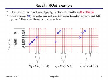
Recall ROM example
- Here are three functions, V2V1V0, implemented
with an 8 x 3 ROM. - Blue crosses (X) indicate connections between
decoder outputs and OR gates. Otherwise there is
no connection.
A2 A1 A0
V2 ?m(1,2,3,4) V1 ?m(2,6,7) V0 ?m(4,6,7)
2
Recall ROM example with shortened notation
- Here is an alternative presentation of the same 8
x 3 ROM, using abbreviated OR gates to make the
diagram neater.
V2 ?m(1,2,3,4) V1 ?m(2,6,7) V0 ?m(4,6,7)
3
Programmable logic arrays
- A ROM is potentially inefficient because it uses
a decoder, which generates all possible minterms.
No circuit minimization is done. - Using a ROM to implement an n-input function
requires - An n-to-2n decoder, with n inverters and 2n
n-input AND gates. - An OR gate with up to 2n inputs.
- The number of gates roughly doubles for each
additional ROM input. - A programmable logic array, or PLA, makes the
decoder part of the ROM programmable too.
Instead of generating all minterms, you can
choose which products (not necessarily minterms)
to generate.
4
A blank 3 x 4 x 3 PLA
- This is a 3 x 4 x 3 PLA (3 inputs, up to 4
product terms, and 3 outputs), ready to be
programmed. - The left part of the diagram replaces the decoder
used in a ROM. - Connections can be made in the AND array to
produce four arbitrary products, instead of 8
minterms as with a ROM. - Those products can then be summed together in the
OR array.
5
Regular K-map minimization
- The normal K-map approach is to minimize the
number of product terms for each individual
function. - For our three functions, this would result in a
total of six different product terms.
V2 V1 V0
V2 ?m(1,2,3,4) V1 ?m(2,6,7) V0 ?m(4,6,7)
6
PLA minimization
- For a PLA, we should minimize the number of
product terms for all functions together. - We could express V2, V1 and V0 with just four
total products
V2 xyz xz xyz V1 xyz xy V0
xyz xy
V2 ?m(1,2,3,4) V1 ?m(2,6,7) V0 ?m(4,6,7)
7
PLA example
- So we can implement these three functions using a
3 x 4 x 3 PLA
A2 A1 A0
xyz
xy
xz
xyz
V2 V1 V0
8
PLA evaluation
- A k x m x n PLA can implement up to n functions
of k inputs, each of which must be expressible
with no more than m product terms. - Unlike ROMs, PLAs allow you to choose which
products are generated. - This can significantly reduce the fan-in (number
of inputs) of gates, as well as the total number
of gates. - However, a PLA is less general than a ROM. Not
all functions may be expressible with the limited
number of AND gates in a given PLA. - In terms of memory, a k x m x n PLA has k address
lines, and each of the 2k addresses references an
n-bit data value. - But again, not all possible data values can be
stored.
9
Summary
- There are two main kinds of random access memory.
- Static RAM costs more, but the memory is faster.
Static RAM is often used to implement cache
memories. - Dynamic RAM costs less and requires less physical
space, making it ideal for larger-capacity
memories. However, access times are also slower. - ROMs and PLAs are programmable devices that can
implement arbitrary functions, which is
equivalent to acting as a read-only memory. - ROMs are simpler to program, but contain more
gates. - PLAs use less hardware, but it requires some
effort to minimize a set of functions. Also, the
number of AND gates available can limit the
number of expressible functions.
10
Datapaths
- Well focus next on computer architecture how
to assemble the combinational and sequential
components weve studied so far into a complete
computer. - Today, well start with the datapath, the part of
the central processing unit (CPU) that does the
actual computations.
11
An overview of CPU design
- We can divide the design of our CPU into three
parts - The datapath does all of the actual data
processing. - An instruction set is the programmers interface
to CPU. - A control unit uses the programmers instructions
to tell the datapath what to do. - Today well look in detail at a processors
datapath, which is responsible for doing all of
the dirty work. - An ALU does computations, as weve seen before.
- A limited set of registers serves as fast
temporary storage. - A larger, but slower, random-access memory is
also available.
12
Whats in a CPU?
- A processor is just one big sequential circuit.
- Some registers are used to store values, which
form the state. - An ALU performs various operations on the data
stored in the registers.
13
Block symbols for registers
- Well use this block diagram to represent an
n-bit register. - There is a data input and a load input signal.
- When Load 1, the data input is stored into the
register. - When Load 0, the register will keep its current
value. - The registers contents are always available on
the output lines, regardless of the Load input. - The clock signal is not shown because it would
make the diagram messy. - Remember that the input and output lines are
actually n bits wide!
14
Register files
- Modern processors have a number of registers
grouped together in a register file. - Much like words stored in a RAM, individual
registers are identified by an address. - Here is a block symbol for a
- 2k x n register file.
- There are 2k registers, so register addresses are
k bits long. - Each register holds an n-bit word, so the data
inputs and outputs are n bits wide.
15
Accessing the register file
- You can read two registers at once by supplying
the AA and BA inputs. The data appears on the A
and B outputs. - You can write to a register by using the DA and D
inputs, and setting WR 1. - These are registers so there must be a clock
signal, even though we usually dont show it in
diagrams. - We can read from the register file at any time.
- Data is written only on the positive edge of the
clock.
D
n
D data
Write
WR
k
D address
DA
Register File
k
k
A address
B address
AA
BA
A data
B data
n
n
A
B
16
Whats inside the register file
- Heres a 4 x n register file. (Well assume a 4 x
n register file for all our examples.)
17
Explaining the register file
- The 2-to-4 decoder selects one of the four
registers for writing. If WR 1, the decoder
will be enabled and one of the Load signals will - be active.
- The n-bit 4-to-1 muxes select the two register
file outputs A and B, based on the inputs AA and
BA. - We need to be able to read two registers at once
because most arithmetic operations require two
operands.
18
The all-important ALU
- The main job of a central processing unit is to
process, or to perform computations....remember
the ALU from way back when? - Well use the following general block symbol for
the ALU. - A and B are two n-bit numeric inputs.
- FS is an m-bit function select code, which picks
one of 2m functions. - The n-bit result is called F.
- Several status bits provide more
- information about the output F
- V 1 in case of signed overflow.
- C is the carry out.
- N 1 if the result is negative.
- Z 1 if the result is 0.
19
ALU functions
- For concrete examples, well use the ALU as its
presented in the textbook. - The table of operations on the right is taken
from page 373. - We use an alternative notation for AND and OR to
avoid confusion with arithmetic operations. - The function select code FS is 5 bits long, but
there are only 15 different functions here.
20
Two questions
- Four registers isnt a lot. What if we need more
storage? - Who exactly decides which registers are read and
written and which ALU function is executed?
21
More Storage We can access RAM also
- Heres a way to connect RAM into our existing
datapath. - To write to RAM, we must give an address and a
data value. - These will come from the registers. We connect A
data to the memorys ADRS input, and B data to
the memorys DATA input. - Set MW 1 to write to the RAM. (Its called MW
to distinguish it from the WR write signal on the
register file.)
D data
Write
WR
D address
DA
Register File
A address
B address
AA
BA
A data
B data
A
B
FS
FS
1
V
ALU
C
N
Z
F
MD
22
Reading from RAM
- To read from RAM, A data must supply the address.
- Set MW 0 for reading.
- The incoming data will be sent to the register
file for storage. - This means that the register files D data input
could come from either the ALU output or the RAM. - A mux MD selects the source for the register
file. - When MD 0, the ALU output can be stored in the
register file. - When MD 1, the RAM output is sent to the
register file instead.
n
D data
Write
WR
D address
DA
Register File
A address
B address
AA
BA
A data
B data
RAM
n
ADRS
DATA
OUT
CS
5V
A
B
WR
MW
FS
FS
0
V
ALU
C
N
Z
F
MD
23
Notes about this setup
- We now have a way to copy data between our
register file and the RAM. - Notice that theres no way for the ALU to
directly access the memoryRAM contents must go
through the register file first. - Here the size of the memory is limited by the
size of the registers with n-bit registers, we
can only use a 2n x n RAM. - For simplicity well assume the RAM is at least
as fast as the CPU clock. (This is definitely
not the case in real processors these days.)
Recommended
