
Chapter 171' MOSFET PowerPoint PPT Presentation
1 / 10
Title: Chapter 171' MOSFET
1
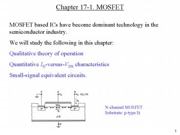
Chapter 17-1. MOSFET
- MOSFET based ICs have become dominant technology
in the semiconductor industry. - We will study the following in this chapter
- Qualitative theory of operation
- Quantitative ID-versus-VDS characteristics
- Small-signal equivalent circuits.
N-channel MOSFET Substrate p-type Si
2
Qualitative discussion NMOS
0 lt VG lt VT VDS small or large no channel, no
current
VG gt VT VDS ? 0 ID increases with VDS
VG gt VT VDS small, gt 0 ID increases with VDS ,
but rate of increase decreases.
VG gt VT VDS ? pinch-off ID reaches a saturation
value, ID,sat The VDS value is called VDS,sat
VG gt VT VDS gt VDS,sat ID does not increase
further, saturation region.
3
ID-VDS characteristics for NMOS derived
fromqualitative discussions
Saturation region
Linear region
4
ID-VDS characteristics expected from a long
channel (?L ltlt L) MOSFET (n-channel), for
various values of VG
5
Threshold voltage for NMOS and PMOS
When VG VT, ?s 2 ?F using equation 16.28, we
get expression for VT.
Ideal n-channel (p-silicon) device both terms
positive
Ideal p-channel (n-silicon) device both terms
negative
?Si / ?ox (?r,Si ?0) / (?r,ox ?0) 11.9 /
3.9 ? 3 ?r,Si 11.9 relative dielectric
constant of Si ?0 absolute dielectric constant
8.85 ? 1012 A s / (V m)
6
Quantitative ID-VDS relationships
Let ? be the potential along the channel
For VG lt VT, Inversion layer charge is zero. For
VG gt VT, Qn(y) ?? QG ? Cox (VG ? ? ? VT)
In general, Jn q ?n n E when the diffusion
current is neglected. Here, current ID is the
same everywhere, but Jn (current density) can
vary from position to position.
7
Device structure, dimension, and coordinate
orientations assumed in the quantitative analysis
8
Quantitative ID-VDS relationships (Shockley model)
since
To find current, we have to multiply the above
with area, but Jny, n, etc. are functions of x
and z. Hence,
Integrating the above equation, and noting that
ID is constant, we get
Since we know expression for Qn(y) in terms of
?, we can integrate this to get ID
9
Quantitative ID-VDS Relationships (cont.)
ID will increase as VDS is increased, but when VG
VDS VT, pinch-off of channel occurs, and
current saturates when VDS is increased further.
This value of VDS is called VDS,sat. i.e.,
VDS,sat VG VT and the current when VDS
VDS,sat is called IDS,sat.
Here, Cox is the oxide capacitance per unit area,
Cox ?ox / xox
10
Example 1
Plot the ID vs. VDS characteristics for an NMOS
with the following parameters
Substrate doping 1016 cm3. Oxide thickness
100 nm Gate width 15??m Gate length 1 ?m.
Assume ?n 500 cm2/(Vs)
Cox ?ox / xox 33.3 nF/cm2
Find Cox
VDS,sat VG VT
Find ID,sat for different values of VG and plot
the graph
Recommended
