
Metrology Roadmap 2000 Update PowerPoint PPT Presentation
1 / 16
Title: Metrology Roadmap 2000 Update
1
Metrology Roadmap2000 Update
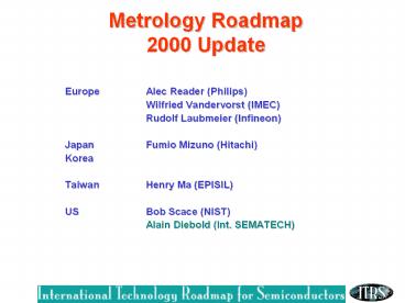
- Europe Alec Reader (Philips)
- Wilfried Vandervorst (IMEC)
- Rudolf Laubmeier (Infineon)
- Japan Fumio Mizuno (Hitachi)
- Korea
- Taiwan Henry Ma (EPISIL)
- US Bob Scace (NIST)
- Alain Diebold (Int. SEMATECH)
2
AGENDA
- 1999 ITRS
- 2000 Review (Why RED?)
- Requirements Tables for 2000 2001
3
1999 Metrology Roadmap Highlights
4
Why are CD Measurement Requirements RED?
- There is no universal metrology solution for all
CD measurements. - e.g., Scatterometry meets Focus-Exposure
precision needs to (70 nm node?) for resist lines
but not for contacts (yet). - 3D info needed for undercut gate, contact, and
other structures. - Precision includes tool matching and near long
term measurement variation.
5
CD-SEM a Potential Solution for Wafer and Mask
/ RD Production
- Barriers and Solutions
- 193 157 nm Resist Damage
- lower dose images
- Precision Improvements
- new nano-tip source
- Depth of Focus
- new SEM concept needed
- Ultimate Limit of CD-SEM
- 5 nm for etched poly Si Gate
From Sato and Mizuno, EIPBN 2000, Palm Springs, CA
6
High Voltage 200 keV is limited to 1 nm
resolution for SE imaging
Many Thanks to David Joy
7
Ultimate limit of CD-SEM
The limit of CD -SEM is based on Secondary
Electron resolution is z the range of
secondary electrons in the material
Many Thanks to David Joy
8
(No Transcript)
9
CD Potential Solutions for Mask and Wafer
60
nm
node
130 / 90
nm
node
40
nm
node
10
CD Potential Solutions for Mask and Wafer
60
nm
node
130 / 90
nm
node
40
nm
node
11
Materials Characterization Enables Process and
Metrology Development
Oxynitride and High k Interfaces
NRA Total N in oxynitride
Dave Muller - Lucent
12
Gate Dielectric Metrology Potential
Solutions Enable High k Development with Existing
Tool
IR or UV for In-Line ?
Desorber New Software w/optical model High k
and Interface
Existing in-line metrology
Next Generation Tool
60
nm
node
130 / 90
nm
node
40
nm
node
Reason for Red is Precision and Tool Matching
13
Interconnect Metrology SolutionsBarrier/Seed Cu
Films
Acoustic ISTS Picosecond acoustics X-ray
reflectivity X-ray fluorescence Non-contact
resistivity
5 Potential Solutions all expected to meet
precision requirements some are extendable to
patterned wafers
14
Metrology New Structures
Vertical Transistor CD is a Film Thickness
Courtesy Rafi Kleiman Lucent
15
2000 and 2001 Changes
- Accelerated Timeline Brings RED closer..
- Developments in some CD measurements push Red out
further for some applications?
16
Metrology Challenges by 2000 ITRS NodeTiming
Brings RED Closer
Recommended
