
Wafer Handling Automation in Semiconductor Manufacturing PowerPoint PPT Presentation
Title: Wafer Handling Automation in Semiconductor Manufacturing
1
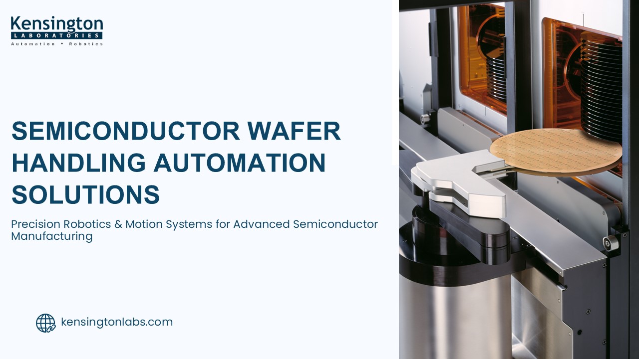
SEMICONDUCTOR WAFER HANDLING AUTOMATION
SOLUTIONS
Precision Robotics Motion Systems for Advanced
Semiconductor Manufacturing
kensingtonlabs.com
2
What is Semiconductor Wafer Handling Automation?
Semiconductor wafer handling automation refers to
robotic systems designed to transport wafers
safely and precisely between different processing
stages within a fabrication facility.
- Automated wafer transfer between tools
- High-precision robotic movement
- Reduced contamination in cleanroom environments
- Consistent wafer positioning and alignment
3
What is a Wafer Handling Robot?
A wafer handling robot is a precision robotic
system used in semiconductor fabs to move wafers
between load ports, process chambers, and
inspection systems.
- High positional accuracy
- Cleanroom-compatible design
- Fast wafer transfer speeds
- Integration with semiconductor equipment
- Benefits
- Increased productivity
- Reduced manual handling
- Improved process reliability
4
Role of Equipment Front-End Modules (EFEM)
The EFEM acts as the interface between wafer
carriers and semiconductor processing equipment.
- Functions
- Carrier docking and wafer loading
- Wafer mapping and identification
- Robotic wafer transfer
- Isolation of the clean process environment
5
Wafer End Effector Technology
A wafer end effector is the robotic tool used to
grip and transport wafers with high precision.
- Common Types
- Vacuum end effectors
- Edge grip end effectors
- Bernoulli end effectors
- Advantages
- Gentle wafer handling
- Reduced contamination risk
- High positioning accuracy
6
Benefits of Wafer Handling Automation
Automation systems significantly improve the
performance and reliability of semiconductor
fabrication processes.
- Key Benefits
- Higher manufacturing throughput
- Improved wafer handling accuracy
- Reduced contamination risks
- Increased equipment uptime
- Scalable semiconductor automation
7
Why Choose Kensington Laboratories
Kensington Laboratories delivers advanced
semiconductor automation solutions designed for
precision, reliability, and efficiency.
- Core Expertise
- Wafer handling robots
- Equipment front-end modules
- Precision motion control systems
- Semiconductor automation engineering
8
THANK YOU
CONTACT INFORMATION
(510) 685-7040
sales_at_kensingtonlabs.com
kensingtonlabs.com
6200 Village Parkway, Dublin, CA 94568
Recommended
