
Precision Interfaces in Wafer Automation PowerPoint PPT Presentation
Title: Precision Interfaces in Wafer Automation
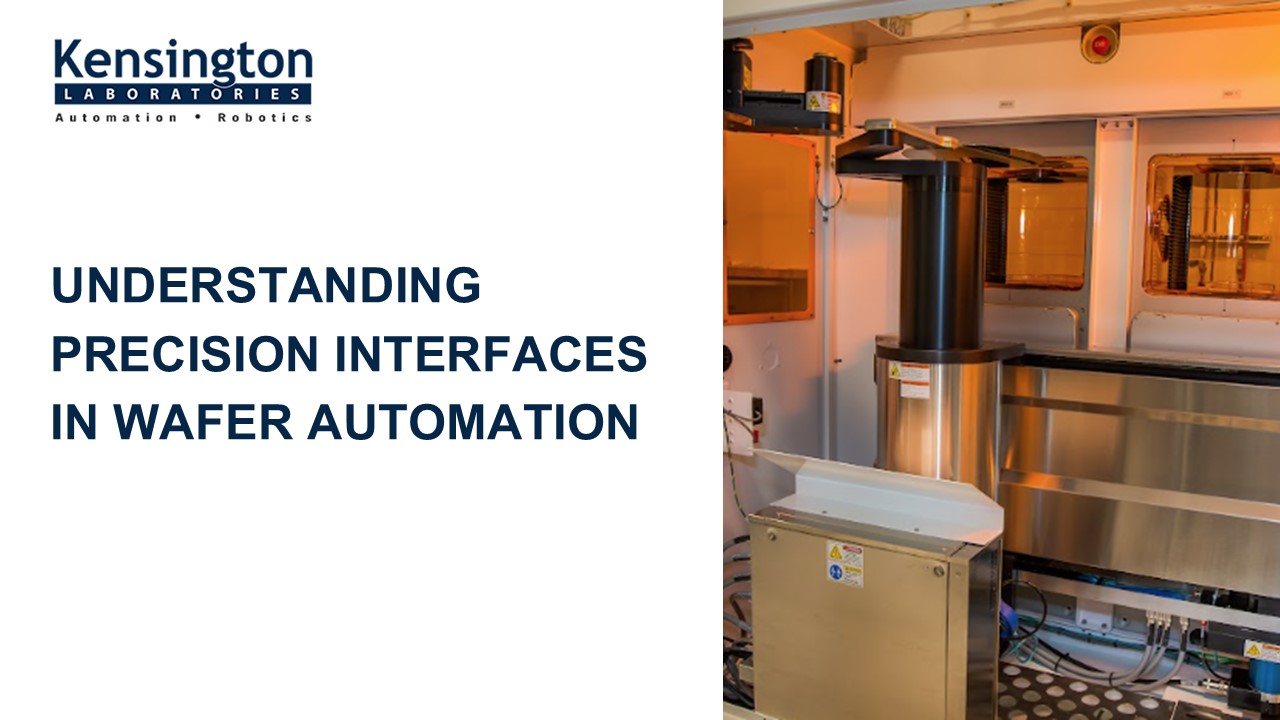
1
UNDERSTANDING PRECISION INTERFACES IN WAFER
AUTOMATION
2
- In automated semiconductor tools, Wafer Handling
End Effector form the controlled contact point
between robotic systems and silicon wafers. - Their design directly influences handling
accuracy, cleanliness, and process reliability. - Core Purpose
- Enable stable wafer pickup and release
- Maintain wafer integrity during robotic motion
- Support repeatable, high-speed automation
3
ENGINEERING CHALLENGES IN WAFER TRANSFER
Automated wafer movement demands extreme control
due to fragile substrates and tight process
tolerances.
KEY CHALLENGES
- Preventing wafer slippage or micro-cracks
- Controlling contact force and pressure
distribution - Avoiding particle generation in cleanroom
environments - Precision interfaces are engineered to balance
holding strength with minimal mechanical stress.
4
INTERFACE TECHNOLOGIES USED IN MODERN TOOLS
Different wafer processes require different
interface mechanisms, selected based on
application sensitivity.
COMMON TECHNOLOGIES
- Vacuum-based contact interfaces
- Edge-support handling mechanisms
- Low-pressure air-assisted (non-contact) designs
- Each approach is optimized for wafer size,
surface condition, and tool integration.
5
DESIGN FACTORS THAT DRIVE PERFORMANCE
High-performance interfaces are defined by both
mechanical design and material science.
PERFORMANCE DRIVERS
- Cleanroom-compatible, low-outgassing materials
- High positional repeatability and flatness
control - Seamless integration with robotic arms and motion
stages - Kensington Laboratories focuses on
precision-machined designs that deliver long-term
stability.
6
VALUE TO ADVANCED SEMICONDUCTOR MANUFACTURING
Precision interfaces play a critical role in
enabling efficient and scalable wafer automation.
OPERATIONAL BENEFITS
- Reduced wafer handling errors
- Improved process consistency
- Higher equipment uptime and yield
- Result
- Reliable wafer transfer interfaces support
next-generation semiconductor manufacturing
demands.
7
THANK YOU
- 1 510-324-0126
- sales_at_kensingtonlabs.com
- 6200 Village Parkway, Dublin
- kensingtonlabs.com
Recommended
