Himanshu Khatri, Lawrence E. Larson PowerPoint PPT Presentation
1 / 1
Title: Himanshu Khatri, Lawrence E. Larson
1
Himanshu Khatri, Lawrence E. Larson Donald
LieDepartment of Electrical and Computer
Engineering Jacobs School of Engineering,
University of California San Diego, CA 92093
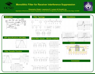
Monolithic Filter for Receiver Interference
Suppression
Motivation
Filter Topology
Simulations
3-pole band pass filter
Inverter transformation
Variation with Q
- Factors affecting the electrical characteristics
of bond wires are - Bond wire quality factor
- Coefficient of mutual coupling
- Self inductance of the bond wire
Merging negative capacitances
Adding bond wire inductances
- TX leakage desensitizes the receiver and cross
modulates with the jammer producing in-band
interference - This requires high linearity (power hungry) LNA
and expensive off-chip SAW filter - Our research aims at a practical approach for
on-chip filtering to eventually replace SAW
filters in some applications
Final Schematic
Variation with L
Variation with k
Requires only on-chip MIM capacitors. No spiral
inductors!
BPF Specifications (WCDMA)
Bond Wire Issues Mutual Coupling
- Rx band 2.11G 2.17G
- Tx band 1.92G 1.98G
- Rx-Tx Selectivity 21dB
- Noise Figure 3dB
- Group Delay Variation 20 nsec
- IIP3 25 dBm
- Coupling between adjacent bond wires within the
section results in frequency translation
Layout
- Coupling across the sections leads to pole
splitting in the pass band
Filter Transfer Function
Chebyshev Eq. Low Pass Filter
Filter Specifications
Bandpass Specification ?center 2.14G ?pass
2.10G Amax -0.5dB ?stop 1.98G Amin -40dB
- Coupling with I/O increases insertion loss
The chip has been sent for fabrication on Jazz
SiGe120 process and is expected to be back in
June 05 for testing.
Chebyshev LP response Opass 1 Amax
-0.5dB Ostop 4.2 Amin -40dB n 3
Conclusion
Solution Ground Shielding Avoid coupling with
I/O and across the sections
A passive filter with low noise can be
constructed using only on-chip MIM capacitors and
bond wire inductors. The simulations show that
such a filter is capable of providing the desired
selectivity with some insertion loss. With high
density capacitors and high quality bond wires
this on-chip filter has the potential to replace
SAW filter.
Pole Frequency Q 2.14 GHz
43.0965 2.14 GHz 43.0965 2.10 GHz
92.149 2.10 GHz 92.149 2.178
GHz 92.149 2.178 GHz 92.149
Pole Frequency Q 0.6265
0.5 1.0689 1.7062 1.0689
1.7062

