
12.2 POWER MOS PowerPoint PPT Presentation
1 / 46
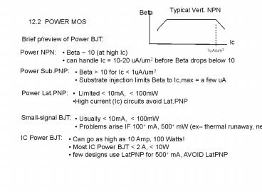
Title: 12.2 POWER MOS
1
Typical Vert. NPN
Beta
12.2 POWER MOS
Brief p/review of Power BJT
Ic
1uA/um2
Power NPN
- Beta 10 (at high Ic)
- can handle Ic 10-20 uA/um2 before Beta drops
below 10
Power Sub.PNP
- Beta gt 10 for Ic lt 1uA/um2
- Substrate injection limits Beta to Ic,max a
few uA
Power Lat.PNP
- Limited lt 10mA, lt 100mW
- High current (Ic) circuits avoid Lat.PNP
Small-signal BJT
- Usually lt 10mA, lt 100mW
- Problems arise IF 100 mA, 500 mW (ex thermal
runaway, needs special layout)
IC Power BJT
- Can go as high as 10 Amp, 100 Watts!
- Most IC Power BJT lt 2 A, lt 10W
- few designs use LatPNP for 500 mA, AVOID LatPNP
2
12.2 POWER MOS
- Advantages of Power MOS over Power BJT
- lack of saturation delay and speed 1 MHz,
- simpler device requirements, lower forward
voltages - drive circuitry capacitive load (Gate), large
currents only during switching transitions - ex) To drive 1-Amp Power MOS average Gate
current (IG, ave) is only
a few mA
- BJT
- saturation delay of 1ms, switching speed upper
limit of 500 kHz - clamping NPN for higher speed costs much
increased forward voltage drops - require constant Base current because beta 10
(_at_high IC) ex) To drive a 1-Amp Power NPN
needs IB 100 mA !
3
Power MOS Large Drain current at very small
VDS, linear region.Here MOS behaves like a
Resistor.
ID k (VGS Vt) VDS k VDS2 / 2 k (VGS
Vt) VDS RDS(on) VDS/ID 1/ k (VGS-Vt)
- on-resistance inversely proportional to k and
Vgst. - typical discrete MOS RDS(on) a few mW.
large sizes - typical Integrated MOS RDS(on) 25 mW 1 W.
restricted sizes - In calc., Metallization and Bond wires affect R
strongly. So, use an empiricaldata RDS(on) vs.
Area
4
Due to Electromigration
Max Temp, heat sink efficiency, Ex) op. at high
Power for lt 10mseconds at a time
Avalanch, punchthrough
5
- Electrical SOA
- Due to Impact Ionization
- Lightly doped Backgate(BG) ? BG debiasing at
large ID ? Forwardbias of S/BG exceeds junction
Turn On voltage ? minority electrons
injectedinto BG travels to D/BG depletion region
? Impact ionization ? more BG debiasing ?
Positive feedback and ID rises dramatically. - Avalanch rating higher the better
- Higher VGS ? higher ID
- Beakdown BVDS falls with rising VGS if
Electrical SOA
?
- Very low avalanch energy rating IF Elec. SOA
- Currents in drift (depletion) region often flow
thru thin filaments of high field spot
(destructive localization)
6
- proper layout to improve electrical SOA
- interdigitated back gate contacts ? some benefit
at the cost of increased area - More compact solution insert interdigitated BG
contact into S contact - Most high V power MOS is elongated annular gate
7
- Thermal runaway in hot spot in parasitic NPN
- Starts same way as Electrical SOA
- High rise of VDS (due to rising ID) starts impact
ionization inD/BG depletion (drift) region ?
injection into BG and BG debiasing ? S/BG
forward ? Parasitic BJT(NPN) ? adds to ID ? loss
of controllt - Avalanche snapback
- D/BG depletion region heats up ? heat spreads
to S/BG junction (EBJ)? locally hot spots in EBJ
conducts more current ? Si melts and destructs!
Electrothermal SOA
- Electrical SOA occursin nS due to Filamentation
- Electrothermal SOA
- Occurs in a few 100 uS.
8
Rapid Transient Overload
- Rsh of Poly about 1,000x Rsh of Metal. Long,
narrow gate finger has significant R. - Rapid ON-OFF signal suffers RCG delay, and MOS
closer to signal src will undergo ON/OFF
beforeMOS farther away can follow. - Progressive turn-ON characteristic can sometimes
lead to local overheating.
Ex) VG rises rapidly ? M1 turns on before M2,
M3, .. Do ? All charge on CL will discharge
throughM1, and large ID will flow for large V. ?
damages M1. Condition rise time lt RCG
V
9
S/D Metallization of Power MOS
S
- Small-signal, interdigitated MOS
G
D
10
S/D Metallization of Power MOS
S
- Small-signal, interdigitated MOS
G
D
- Power MOS, interdigitated,
G
M-1
11
S/D Metallization of Power MOS
S
- Small-signal, interdigitated MOS
G
D
- Power MOS, interdigitated, S/D Metallization
S/D metallization contact in interdigitatedM-1,
connected thru VIA to M-2 bus
M-1
G
M-1 with S/D contacts
M-1 gate
12
12.2.2 Conventional MOS Power Transistor
- generally, no benefit from ballasting. The same
finger layout as small-signal - RDS(on) increases 50 as T25C ? 125C
fluctuates 30 over process. - RM SD metallization, difficult to calc.
because geometry dep. ? use measured R - ? measure RDS(on) vs. drawn Area Ad.
RDS(on) 1 / k(VGS-Vt) RM
- Specific on-resistance RSP RSP Ad RDS(on)
W mm2 - difficult because RSP should not contain R due
to bondwires and leadframe - depends on device Area and Aspect Ratio ? valid
only for area 2x 3x range
13
12.2.2 Conventional MOS Power Transistor
Rectangular Device
- double-level metal for S/D for maximum
metallization M-1 interdigitate ? maximum
contacts M-2 bus ? draws IS,D thru VIAs - Voltage drop VSM along the S finger VDM along
D finger
14
12.2.2 Conventional MOS Power Transistor
Rectangular Device
- double-level metal for S/D for maximum
metallization M-1 interdigitate ? maximum
contacts M-2 bus ? draws IS,D thru VIAs - Voltage drop VSM along the S finger VDM along
D finger
G
M-1 with S/D contacts
15
12.2.2 Conventional MOS Power Transistor
16
12.2.2 Conventional MOS Power Transistor
Rectangular Device
- Current Flow directions in S/D Fingers
Better than (A) and (C )
- Common arrangement
- Connecting to nearby Bondpad
- produce excessive voltage drop
- Uneven distribution of currents
- better arrangement than (A)
- more even distribution of current
- lower total R than (A)
- not have to flow full length of bus
- minimizes R
- uneven current distribution
17
12.2.2 Conventional MOS Power Transistor
Diagonal Device
- Rectangular Bus width const Current not
constant. - Diagonal Tapered Buses more uniform current
in fingers. More difficult to layout. - Many designers prefer Fig.12.18(B) over Tapered
Bus (Fig.12.19)
18
12.2.2 Conventional MOS Power Transistor
Computation of RM
For Fig.12.18B, assuming each finger conducts
equal current, linear increase of current in M-2
buses, neglecting voltage variation across M-2
bus width
RM B2 RS1/(2W NDL) A RS12 / (2W ND) H
RS2/2B
Where, ND of Drain fingers RS1 sheet
resistance of M-1 RS2 sheet resistance of
M-2 RS12 sheet resistance of parallel
combination of M-1 and M-2 A, B, W, L, H
defined in Fig.12-16
19
12.2.2 Conventional MOS Power Transistor
Computation of RM
For Fig.12.18B, assuming each finger conducts
equal current, linear increase of current in M-2
buses, neglecting voltage variation across M-2
bus width
RM B2 RS1/(2W NDL) A RS12 / (2W ND) H
RS2/2B
Where, ND of Drain fingers RS1 sheet
resistance of M-1 RS2 sheet resistance of
M-2 RS12 sheet resistance of parallel
combination of M-1 and M-2 A, B, W, L, H
defined in Fig.12-16
Optimum width of M-2 bus, Fig.12.18B for a single
finger B L RS12/RS1 L t1/(t1t2) if M-1
and M-2 are same material
20
12.2.2 Conventional MOS Power Transistor
Other Factors
- R of long, narrow gate fingers substantially
slows switching of large Power T - Connecting both ends of G R ? ¼ R
- BG contacts and Guard ringsBG (interdigitated or
distributed) to preventBG debiasing (causes
S/BG forward bias,more minority carrier
injection into BG)Guard rings to intercept
minority carriers.
21
12.2.2 Conventional MOS Power Transistor
Other Factors
- To monitor the Power T operation use small
Sense transistor. - Sense T has same G and S as main T, but has
separate D. - Put Sense T in the middle of one-side (1), both
sides (2), middle of all sides (4), etc. - Average of these Sense Ts average op.
conditions of Power T.
22
12.2.2 Conventional MOS Power Transistor
Other Factors
23
DMOSDouble-diffused MOS
12.2.3 DMOS Transistor
- High V transistors need short/heavily doped BG
wide/light ly doped Drift regions. - ? done by diffusion of BG into Drift region. ?
Double Diffused
24
DMOSDouble-diffused MOS
12.2.3 DMOS Transistor
- High V transistors need short/heavily doped BG
wide/light ly doped Drift regions. - ? done by diffusion of BG into Drift region. ?
Double Diffused
Large I, large V
Large Current
Large Voltage
25
DMOSDouble-diffused MOS
12.2.3 DMOS Transistor
26
12.2.3 DMOS Transistor
1. Both As and B implant ? Drive-in diffusion ? B
diffuses faster, farther than As
27
12.2.3 DMOS Transistor
2. Moderately B-doped
1. Both As and B implant ? Drive-in diffusion ? B
diffuses faster, farther than As
28
12.2.3 DMOS Transistor
N Sub as the Drain contactfor Discrete Vertical
DMOS
2. Moderately B-doped
3. lightly-dopedN-epi
1. Both As and B implant ? Drive-in diffusion ? B
diffuses faster, farther than As
29
12.2.3 DMOS Transistor
Current flow
N Sub as the Drain contactfor Discrete Vertical
DMOS
2. Moderately B-doped
3. lightly-dopedN-epi
1. Both As and B implant ? Drive-in diffusion ? B
diffuses faster, farther than As
Lchannel length Surface, difference betweenAs
and B diffusion lengths.
30
12.2.3 VDMOS Transistor
A large VDMOS Power device composed of an array
of DMOS Cells or DMOS Strips
31
12.2.3 VDMOS Transistor
A large VDMOS Power device composed of an array
of DMOS Cells or DMOS Strips
32
Lateral DMOS Transistor (LDMOS)
- Most IC Power Tran
- Lseparation betweenD and BG contacts
- NBLnot reqd, if presentjust to min. sub.
Injection - S/BG shorted (P plugcontacts BG, next to
NSource (P/N)
33
Lateral DMOS Transistor (LDMOS)
- Most IC Power Tran
- Lseparation betweenD and BG contacts
- NBLnot reqd, if presentjust to min. sub.
Injection - S/BG shorted (P plugcontacts BG, next to
NSource (P/N)
34
Lateral DMOS Transistor (LDMOS)
- Most IC Power Tran
- Lseparation betweenD and BG contacts
- NBLnot reqd, if presentjust to min. sub.
Injection - S/BG shorted (P plugcontacts BG, next to
NSource (P/N)
Channel
35
Lateral DMOS Transistor (LDMOS)
- NBL is absent
- Nwell is fully depleted and
- S must connect to Sub potential
- Positioned between LOAD and GND return
- Is called LSD, Low-side-drive
- Has a higher voltage rating
Substrate
Supply Rail (VDD)
D
G
High-side Drive (HSD)
BG
S
Out
D
G
Low-Side Drive (LSD)
BG
S
Ground Rail (GND) Sub
36
Lateral DMOS Transistor (LDMOS)
Substrate
- NBL is present
- NBL prevents punchthruof Nwell, but increases
E-field by containing depl region - S and Sub can be at differentPotential, and thus
- Can position between LOADand Positive rail, so
called - HSD, High-Side-Drive
- Has a lower voltage rating
Supply Rail (VDD)
D
G
High-side Drive (HSD)
BG
S
Out
D
G
Low-Side Drive (LSD)
BG
S
Ground Rail (GND) Sub
37
RESURF Transistor REduced SURface Field transistor
- Consider PN junction the depletion Given the
junction bias V, the depletion width Wd is set
to expose enough charge to support the bias.
Wd larger ? E-field smaller ? higher Vbr - By limiting vertical depletion, the lateral
depletion can be forced to expand further so that
the combined vertical depletion lateral
depletion can support the junction bias. ? the
expanded lateral depletion ? decreased surface
E-field.
38
RESURF Transistor REduced SURface Field transistor
- Conventional structure uses Deep wells (or
epilayers) to keep the drain/sub depletion away
from Active region. - recent development Deep drains are unnecessary
shallow wells actually reduces surface field
(for higher V operation.
- A high V applied to N-tank ? depletion forms in
N-tank/P-region ? epi/sub depl extends XV,
vertically ?epi/iso extends Xlat, laterally ?
But, the shaded region is already depleted by
epi/sub depl ? thus,the epi/iso depl must extend
further into N-epi in order to uncover needed
ionized donors ? increase inLateral Depl width
leads to Reduced lateral surface E-field. E
1/(Xlat DL) - SO, shallower Nepi gives wider lateral Depletion
into Nepi which gives lower Surface Field. ?
needsthe vertical depl region and lateral depl
region to interact with each other.
39
RESURF Transistor REduced SURface Field transistor
- Conventional structure uses Deep wells (or
epilayers) to keep the drain/sub depletion away
from Active region. - recent development Deep drains are unnecessary
shallow wells actually reduces surface field
(for higher V operation.
- A high V applied to N-tank ? depletion forms in
N-tank/P-region ? epi/sub depl extends XV,
vertically ?epi/iso extends Xlat, laterally ?
But, the shaded region is already depleted by
epi/sub depl ? thus,the epi/iso depl must extend
further into N-epi in order to uncover needed
ionized donors ? increase inLateral Depl width
leads to Reduced lateral surface E-field. E
1/(Xlat DL) - SO, shallower Nepi gives wider lateral Depletion
into Nepi which gives lower Surface Field. ?
needsthe vertical depl region and lateral depl
region to interact with each other.
40
RESURF Transistor REduced SURface Field transistor
- Conventional structure uses Deep wells (or
epilayers) to keep the drain/sub depletion away
from Active region. - recent development Deep drains are unnecessary
shallow wells actually reduces surface field
(for higher V operation.
- A high V applied to N-tank ? depletion forms in
N-tank/P-region ? epi/sub depl extends XV,
vertically ?epi/iso extends Xlat, laterally ?
But, the shaded region is already depleted by
epi/sub depl ? thus,the epi/iso depl must extend
further into N-epi in order to uncover needed
ionized donors ? increase inLateral Depl width
leads to Reduced lateral surface E-field. E
1/(Xlat DL) - SO, shallower Nepi gives wider lateral Depletion
into Nepi which gives lower Surface Field. ?
needsthe vertical depl region and lateral depl
region to interact with each other.
41
Low-Side-Drive RESURF DMOS
42
Low-Side-Drive RESURF DMOS
- This Nwell region under P-body depletes entirely
thru. - Lateral depletion around Nwell/P-ei increases per
RESURF effect - Reduces E-field _at_ Drain sidewall ? increases Vbr
- Similar effect at D/BG sidewall
43
Low-Side-Drive RESURF DMOS
- This Nwell region under P-body depletes entirely
thru. - Lateral depletion around Nwell/P-ei increases per
RESURF effect - Reduces E-field _at_ Drain sidewall ? increases Vbr
- Similar effect at D/BG sidewall
44
Low-Side-Drive RESURF DMOS
- Electrical SOA limitation (historically)
- Kirk effect caused high E-field spot to move
from D/BG to NW/extrinsic D - Use N-channel-stop implant to moderately dope
NW/extrinsic D - this stops the high E-field. Adaptive RESURF
45
Modern LDMOS
- Last few years of development made LDMOS offer
extremely good device characteristics today - Best characteristics available
- High Vbr
- Square or near-square SOA
- Low Rsp (specific ON resistance)
- Now, they are the best High-V Power Transistor
for IC today
46
DMOS NPN
Recommended
