
Multi%20Cycle%20CPU PowerPoint PPT Presentation
Title: Multi%20Cycle%20CPU
1
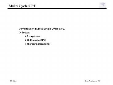
Multi Cycle CPU
- Previously built a Single Cycle CPU.
- Today
- Exceptions
- Multi-cycle CPU
- Microprogramming
2
Mid-term Review Discussion Session
- Peterson Hall 104
- Tue 2-3 pm
- Tue 3-4 pm
3
The Story so far
- Instruction Set Architectures
- Performance issues
- 2s complement, Addition, Subtraction
- Multiplication, Division, Floating Point numbers
- ALUs
- Single Cycle CPU
- Exceptions
- Multicycle CPU datapath control
- Microprogramming
4
Alternative Architectures
- Design alternative
- provide more powerful operations
- goal is to reduce number of instructions executed
- danger is a slower cycle time and/or a higher CPI
- Sometimes referred to as RISC vs. CISC
- virtually all new instruction sets since 1982
have been RISC - VAX minimize code size, make assembly language
easy instructions from 1 to 54 bytes long! - Well look at Pentium, UltraSparc and JVM
5
Pentium
6
Java VM
- Most instr one byte
- ADD
- POP
- One byte arg
- ILOAD IND8
- BIPUSH CON8
- Two byte arg
- SIPUSH CON16
- IF_ICMPEQ OFFSET16
- Type int, signed int etc.
7
UltraSparc
8
Exceptions
or Oops!
9
Exceptions
- There are two sources of non-sequential control
flow in a processor - explicit branch and jump instructions
- exceptions
- Branches are synchronous and deterministic
- Exceptions are typically asynchronous and
non-deterministic - Guess which is more difficult to handle?
arithmetic overflow divide by zero I/O device
signals completion to CPU user program invokes
the OS memory parity error illegal
instruction timer signal
- exceptions as any unexpected change in control
flow - interrupts as any externally-caused exception
- Literature is not consistent
10
Exceptions
- The machine weve been designing in class can
generate two types of exceptions. - arithmetic overflow
- illegal instruction
- On an exception, we need to
- save the PC (invisible to user code)
- record the nature of the exception/interrupt
- transfer control to OS
System Exception Handler
user program
Exception
return from exception
11
Exceptions
- Interrupts
- caused by external events
- asynchronous to program execution
- may be handled between instructions
- simply suspend and resume user program
- Traps/Exceptions
- caused by internal events
- exceptional conditions (overflow)
- errors (parity)
- faults (non-resident page)
- synchronous to program execution
- condition must be remedied by the handler
- instruction may be retried or simulated and
program continued or program may be aborted
- MIPS architecture defines the instruction as
having no effect if the instruction causes an
exception. - When we get to virtual memory we will see that
certain classes of exceptions must prevent the
instruction from changing the machine state. - This aspect of handling exceptions becomes
complex and potentially limits performance gt why
it is hard
12
Exceptions
Addressing the Exception Handler
- Traditional Approach Interupt Vector
- PC lt- MEM IV_base cause 00
- 370, 68000, Vax, 80x86, . . .
- RISC Handler Table
- PC lt IT_base cause 0000
- saves state and jumps
- Sparc, PA, M88K, . . .
- MIPS Approach fixed entry
- PC lt EXC_addr
- Actually very small table
- RESET entry
- TLB
- other
handler entry code
iv_base
cause
13
Exceptions
Saving State
- Push it onto the stack
- Vax, 68k, 80x86
- Save it in special registers
- MIPS EPC, BadVaddr, Status, Cause
- Shadow Registers
- M88k
- Save state in a shadow of the internal pipeline
registers
Significant component of interrupt response time
14
Exceptions
- For our MIPS-subset architecture, we will add two
registers - EPC a 32-bit register to hold the users PC
- Cause A register to record the cause of the
exception - well assume undefined inst 0, overflow 1
- We will also add three control signals
- EPCWrite (will need to be able to subtract 4 from
PC) - CauseWrite
- IntCause
- We will extend PCSource multiplexor to be able to
latch the interrupt handler address into the PC.
15
Exceptions
CauseWrite
Cause
IntCause
16
Exceptions Creating a Control line
- Regs
- EPC
- Cause
- control signals
- EPCWrite (subtract 4 from PC)
- CauseWrite
- IntCause
Instructionlt310gt
Inst Memory
lt2125gt
lt2125gt
lt1620gt
lt1115gt
lt015gt
Adr
Op
Fun
Imm16
Rd
Rs
Rt
Control
Exception Signals
ALUctr
MemtoReg
MemWr
nPC_sel
ALUSrc
RegDst
ExtOp
RegWr
Equal
DATA PATH
17
Exceptions Creating the data path
- Regs
- EPC
- Cause
- control signals
- EPCWrite (subtract 4 from PC)
- CauseWrite
- IntCause
- Extend PCSource MUX to include jump address from
int-table
Ideal Instruction Memory
Instruction
Rd
Rs
Rt
Imm
5
5
5
16
Instruction Address
A
Data Address
32
Rw
Ra
Rb
32
Ideal Data Memory
32
32 32-bit Registers
Next Address
Data In
B
Clk
Clk
32
18
CPU
Multi Cycle CPU
19
CPU
The Big Picture Where are We Now?
- The Five Classic Components of a Computer
- Datapath Design, then Control Design
Processor
Input
Memory
Output
20
Recap Processor Design is a Process
- Bottom-up
- assemble components in target technology to
establish critical timing - Top-down
- specify component behavior from high-level
requirements - Iterative refinement
- establish partial solution, expand and improve
Instruction Set Architecture
gt
processor
datapath
control
Reg. File
Mux
ALU
Reg
Mem
Decoder
Sequencer
Cells
Gates
21
CPU The single cycle
Execute
Decode
Fetch
Fetch
Store
Next
Execute an entire instruction
Design hardware for each of these steps!!!
22
CPU Clocking
Clk
Setup
Hold
Setup
Hold
Dont Care
- All storage elements are clocked by the same
clock edge
23
CPU Main Control
PLA Implementation of the Main Control
RegWrite
ALUSrc
RegDst
MemtoReg
MemWrite
Branch
Jump
ExtOp
ALUoplt2gt
ALUoplt1gt
ALUoplt0gt
24
CPU Main Control
OPcode
Control Logic / Store (PLA, ROM)
Decode
microinstruction
Conditions
Instruction
Control Points
Datapath
- In our single-cycle processor, each instruction
is realized by exactly one control command or
microinstruction - in general, the controller is a finite state
machine - microinstruction can also control sequencing (see
later)
25
CPU Abstract View of a single cycle processor
Main Control
op
ALU control
fun
ALUSrc
Equal
ExtOp
MemRd
MemWr
MemWr
RegDst
RegWr
nPC_sel
ALUctr
Reg. Wrt
ALU
Register Fetch
Ext
Mem Access
PC
Instruction Fetch
Next PC
Result Store
Data Mem
- looks like a FSM with PC as state
26
CPU Why is a CPI1 processor bad?
Arithmetic Logical
PC
Reg File
Inst Memory
ALU
setup
mux
mux
Load
PC
Inst Memory
ALU
Data Mem
Reg File
setup
mux
mux
Critical Path
Store
PC
Inst Memory
ALU
Data Mem
Reg File
mux
Branch
PC
Inst Memory
cmp
Reg File
mux
- Long Cycle Time
- All instructions take as much time as the slowest
- Real memory is not so nice as our idealized
memory - cannot always get the job done in one (short)
cycle
27
CPU Why is a CPI1 processor bad?
Goal balance amount of work done each cycle.
I cache Decode, R-Read ALU PC update D cache R-Write Total
R-type 1 1 .9 - - .8 3.7
Load 1 1 .9 - 1 .8 4.7
Store 1 1 .9 - 1 - 3.9
beq 1 1 .9 .1 - - 3.0
- Load needs 5 cycles
- Store and R-type need 4
- beq needs 3
28
CPU Reducing Cycle Time
- Cut combinational dependency graph and insert
register / latch - Do same work in two fast cycles, rather than one
slow one
storage element
storage element
Acyclic Combinational Logic (A)
Acyclic Combinational Logic
gt
storage element
Acyclic Combinational Logic (B)
storage element
storage element
29
CPU Building blocks
CarryIn
- Adder
- MUX
A
32
Sum
Adder
32
B
Carry
32
Select
A
32
MUX
Y
32
B
32
OP
A
32
Result
ALU
32
B
32
30
CPU Building blocks
- Building a 64-bit adder from 2x32-bit adders
- Speed of addition?
- For one ADD?
- For consecutive ADDS?
31
Multicycle CPU Individual operations
- Next address logic
- PC lt branch ? PC offset PC 4
- Instruction Fetch
- InstructionReg lt MemPC
- Register Access
- A lt Rrs
- ALU operation
- R lt A B
Control
MemRd
RegDst
MemWr
RegWr
MemWr
nPC_sel
ALUctr
ALUSrc
ExtOp
Reg. File
Exec
Operand Fetch
Mem Access
Instruction Fetch
PC
Next PC
Result Store
Data Mem
32
Multicycle CPU Partitioning Time
- Five execution steps (some instructions use
fewer) - IF Instruction Fetch
- ID Instruction Decode ( register fetch add
PCimmed) - EX Execute
- Mem Memory access
- WB Write-Back into registers
- IF ID
EX Mem WB
I cache Decode, R-Read ALU PC update D cache R-Write Total
R-type 1 1 .9 - - .8 3.7
Load 1 1 .9 - 1 .8 4.7
Store 1 1 .9 - 1 - 3.9
beq 1 1 .9 .1 - - 3.0
33
Multicycle CPU Steps
Note Reuse of ALU
IF ID
Ex Mem WB
34
Multicycle CPU
Partitioning the CPI1 Datapath
- Add registers between smallest steps
MemRd
RegDst
MemWr
RegWr
MemWr
nPC_sel
ALUSrc
ExtOp
ALUctr
Reg. File
Exec
Operand Fetch
Mem Access
Instruction Fetch
PC
Next PC
Result Store
Data Mem
35
Multicycle CPU
Cycle 1
Cycle 2
Clk
Single Cycle Implementation
Load
Store
Waste
Cycle 1
Cycle 2
Cycle 3
Cycle 4
Cycle 5
Cycle 6
Cycle 7
Cycle 8
Cycle 9
Cycle 10
Clk
Multiple Cycle Implementation
Load
Store
R-type
36
Multicycle CPU Instruction Types
37
Multicycle CPU Sharing Hardware
IR lt- MemPC
A lt- Rrs Blt Rrt
S lt A B
S lt A SX
S lt A or ZX
S lt A SX
M lt MemS
MemS lt- B
Rrd lt S PC lt PC4
Rrd lt M PC lt PC4
Rrt lt S PC lt PC4
PC lt PC4
PC lt PC4
PC lt PCSX
- Example memory is used twice, at different times
- Ave mem access per inst 1 Flw Fsw 1.3
- if CPI is 4.8, imem utilization 1/4.8, dmem
0.3/4.8 - We could reduce HW without hurting performance
- extra control
38
Multicycle CPU Sharing Functional Units
- Reuse
- ALU
- Memory
- Need more
- Muxing
- Control
Single ALU, Common data and instruction memory
datapath
39
Multicycle CPU Adding State Elements
- Since we reuse logic (e.g. ALU), we need to store
results between states - Need extra registers when
- signal is computed in one clock cycle and used in
another, AND - the inputs to the combinational circuit can
change before the signal is written into a state
element.
40
Multicycle CPU Adding State Elements
IF ID
Ex Mem WB
41
Multicycle CPU The Full Multi-Cycle
Implementation
42
Cycle 1 Instruction Fetch
Datapath IR MemoryPC, PC PC 4 (may be
revised later) Control IorD0, MemRead1,
MemWr0, IRwrite1, ALUsrcA0, etc
43
Cycle 1 Instruction Decode
A RegisterIR25-21 B RegisterIR20-16 AL
Uout PC (sign-extend (IR15-0) ltlt 2)
44
Cycle 2 Instruction Decode RegFetch
- A RegIR25-21
- B RegIR20-16
- ALUout PC (sign-extend (IR15-0) ltlt 2)
- We compute target address even though we dont
know if it will be used - Operation may not be branch
- Even if it is, branch may not be taken
- Why?
- Everything up to this point must be
instruction-independent, because we havent
decoded the instruction. - The ALU, the (incremented) PC, and the immed
field are now all available
45
Cycle 3 for beq EXecute
A
ALU out
B
- In cycle 1, PC was incremented by 4
- In cycle 2, ALUout was set to branch target
- This cycle, we conditionally reset PC if (AB)
PCALUout
46
Cycle 3 R-type Instruction
- Cycle 3 (EXecute)
- ALUout A op B
- Cycle 4 (WriteBack)
- RegIR15-11 ALUout
- R-type instruction is finished
47
Cycle 3 R-type Instruction
A
B
Cycle 3 ALUout A op B Cycle 4
RegIR15-11 ALUout
48
Cycle 4 R-type Instruction
A
ALU out
B
Cycle 3 ALUout A op B Cycle 4
RegIR15-11 ALUout
49
Multicycle CPU The datapath
MemToReg
RegWr
RegDst
MemWr
MemRd
nPC_sel
ALUctr
ALUSrc
ExtOp
Equal
Reg. File
Ext ALU
A
Reg File
R
PC
IR
Next PC
B
Mem Access
M
Data Mem
Instruction Fetch
Result Store
Operand Fetch
- Extra Registers
- IR
- A,B
- R ( sometimes called S or ALUout)
- M
50
Multicycle CPU The datapath
inst Logical Register Transfers ADDU Rrd lt
Rrs Rrt PC lt PC 4
- Logical Register Transfer
- Physical Register Transfers
inst Physical Register Transfers IR lt
MEMpc ADDU Alt Rrs B lt Rrt S lt A
B Rrd lt S PC lt PC 4
Equal
Reg. File
Reg File
Exec
IR
PC
Next PC
Inst. Mem
Mem Access
Data Mem
51
Multicycle CPU The datapath
inst Logical Register Transfers ORI Rrt lt
Rrs OR zx(Im16) PC lt PC 4
- Logical Register Transfer
- Physical Register Transfers
inst Physical Register Transfers IR lt
MEMpc ADDU Alt Rrs B lt Rrt S lt ( A or
ZeroExt(Im16) ) Rrt lt S PC lt PC 4
Equal
Reg. File
Reg File
Exec
IR
PC
Next PC
Inst. Mem
Mem Access
Data Mem
52
Multicycle CPU The datapath
inst Logical Register Transfers LW Rrt lt
MEM(Rrs sx(Im16) PC lt PC 4
- Logical Register Transfer
- Physical Register Transfers
Equal
Reg. File
Reg File
Exec
IR
PC
Next PC
Inst. Mem
Mem Access
Data Mem
53
Multicycle CPU The datapath
inst Logical Register Transfers SW MEM(Rrs
sx(Im16) lt Rrt PC lt PC 4
- Logical Register Transfer
- Physical Register Transfers
inst Physical Register Transfers IR lt
MEMpc SW Alt Rrs B lt Rrt S lt A
SignEx(Im16) MEMS lt B PC lt PC 4
Equal
Reg. File
Reg File
Exec
IR
PC
Next PC
Inst. Mem
Mem Access
Data Mem
54
Multicycle CPU The datapath
inst Logical Register Transfers BEQ if Rrs
Rrt then PC lt PC sx(Im16) 00 else PC
lt PC 4
- Logical Register Transfer
- Physical Register Transfers
inst Physical Register Transfers IR lt
MEMpc BEQEq PC lt PC 4
inst Physical Register Transfers IR lt
MEMpc BEQEq PC lt PC sx(Im16) 00
Equal
Reg. File
Reg File
Exec
IR
PC
Next PC
Inst. Mem
Mem Access
Data Mem
55
Multicycle CPU Summary
56
Multicycle CPU Mid-term alert !!
- How many cycles will it take to execute this
code? lw t2, 0(t3) lw t3, 4(t3) beq
t2, t3, Label assume not add t5, t2,
t3 sw t5, 8(t3)Label ... - What is going on during the 8th cycle of
execution? - In what cycle does the actual addition of t2 and
t3 takes place?
57
Multicycle CPU Sharing Hardware
Princeton Organization
A-Bus
B Bus
A
Reg File
IR
P C
next PC
S
Mem
B
ZX
SX
W-Bus
- Single memory for instruction and data access
- memory utilization -gt 1.3/4.8
- In this case our state diagram does not change
- several additional control signals
- must ensure each bus is only driven by one source
on each cycle
58
Multicycle CPU Control Line Timing
Cycle 1
Cycle 2
Cycle 3
Cycle 4
Cycle 5
Cycle 6
Cycle 7
Cycle 8
Cycle 9
Cycle 10
Clk
Load
Store
R-type
IRWrite
59
Review Finite State Machines
- Finite state machines
- a set of states and
- next state function (determined by current state
and the input) - output function (determined by current state and
possibly input) - Well use a Moore machine (output based only on
current state)
60
Multicycle CPU Control
If (State Instruction Fetch) IRWrite
1 // All other signals are 0 State Operand
Fetch
If (State Execute InstructionOpCode BEQ
) // Do your thing..
ControlOutput f(State, OpCode) NextState
f(State, OpCode)
61
Multicycle CPU Our basic FSM
Instruction fetch
Decode and Register Fetch
R-type instructions
Jump instruction
Memory instructions
Branch instructions
62
Multicycle CPU Control
instruction fetch
IR lt MEMPC
A lt Rrs B lt Rrt
decode / operand fetch
LW
BEQ Equal
R-type
ORi
SW
BEQ Equal
PC lt PC SX 00
PC lt PC 4
S lt A fun B
S lt A or ZX
S lt A SX
S lt A SX
Execute
M lt MEMS
MEMS lt B PC lt PC 4
Memory
Rrd lt S PC lt PC 4
Rrt lt S PC lt PC 4
Rrt lt M PC lt PC 4
Write-back
63
Multicycle CPU Control
Number of states? Number of bits for state?
64
Multicycle CPU Control Assigning States
instruction fetch
IR lt MEMPC
0000
decode
A lt Rrs B lt Rrt
0001
LW
BEQ Equal
R-type
ORi
SW
BEQ Equal
PC lt PC SX 00
Execute
PC lt PC 4
S lt A fun B
S lt A or ZX
S lt A SX
S lt A SX
0100
0110
1000
0011
1011
0010
Memory
M lt MEMS
MEMS lt B PC lt PC 4
1001
1100
Rrd lt S PC lt PC 4
Rrt lt S PC lt PC 4
Rrt lt M PC lt PC 4
Write-back
0101
0111
1010
65
Multicycle CPU Detailed control spec.
State Op field Eq Next IR PC Ops Exec Mem Write-B
ack en sel A B Ex Sr ALU S R W M M-R Wr
Dst
0000 ?????? ? 0001 1 0001 BEQ 0 0011 1
1 0001 BEQ 1 0010 1 1 0001 R-type x 0100 1
1 0001 orI x 0110 1 1 0001 LW x 1000 1
1 0001 SW x 1011 1 1 0010 xxxxxx x 0000 1
1 0011 xxxxxx x 0000 1 0 0100 xxxxxx x 0101
0 1 fun 1 0101 xxxxxx x 0000 1 0 0
1 1 0110 xxxxxx x 0111 0 0 or
1 0111 xxxxxx x 0000 1 0 0 1
0 1000 xxxxxx x 1001 1 0 add
1 1001 xxxxxx x 1010 1 0 0 1010
xxxxxx x 0000 1 0 1 1
0 1011 xxxxxx x 1100 1 0 add
1 1100 xxxxxx x 0000 1 0 0 1
R
ORi
LW
SW
66
Multicycle CPU Implementation styles
- ROM "Read Only Memory"
- values of memory locations are fixed ahead of
time - A ROM can be used to implement a truth table
- if the address is m-bits, we can address 2m
entries in the ROM. - our outputs are the bits of data that the address
points to. - 2m is the "height", and n is the "width"
0 0 0 0 0 1 1 0 0 1 1 1 0 0 0 1 0 1 1 0 0 0 1 1 1
0 0 0 1 0 0 0 0 0 0 1 0 1 0 0 0 1 1 1 0 0 1 1
0 1 1 1 0 1 1 1
67
Multicycle CPU Implementation styles
- How many inputs are there? 6 bits for opcode, 4
bits for state 10 address lines (i.e., 210
1024 different addresses) - How many outputs are there? 16 datapath-control
outputs, 4 state bits 20 outputs - ROM is 210 x 20 20K bits (and a rather
unusual size) - Rather wasteful, since for lots of the entries,
the outputs are the same i.e., opcode is often
ignored
68
Multicycle CPU Implementation styles
- Break up the table into two parts 4 state bits
tell you the 16 outputs, 24 x 16 bits of
ROM 10 bits tell you the 4 next state bits,
210 x 4 bits of ROM Total 4.3K bits of ROM - PLA is much smaller can share product terms
only need entries that produce an active
output can take into account don't cares - Size is (inputs product-terms) (outputs
product-terms) For this example
(10x17)(20x17) 460 PLA cells - PLA cells usually about the size of a ROM cell
(slightly bigger)
69
Multicycle CPU Implementation styles
PLA Implementation
IRWrite (!S0 !S1 !S2 !S3)
NS0 ( S3..0 0000) ( S3..0 0110 )
( S3..0 1001 OP5..0000010 )
() ()
70
Microprogramming
- Control is the hard part of processor design
- Datapath is fairly regular and well-organized
- Memory is highly regular
- Control is irregular and global
- Consider the FSM in case of 100s of instructions
!!!
- FSMs get unmanageable quickly as they grow.
- hard to specify
- hard to manipulate
- error prone
- hard to visualize
- The state digrams that arise define the
controller for an instruction set processor are
highly structured - Use this structure to construct a simple
microsequencer - Control reduces to programming this very simple
device - microprogramming
71
Microprogramming
Microprogramming A Particular Strategy for
Implementing the Control Unit of a processor by
"programming" at the level of register transfer
operations Microarchitecture Logical structure
and functional capabilities of the hardware as
seen by the microprogrammer
Historical Note IBM 360 Series first to
distinguish between architecture organization
Same instruction set across wide range of
implementations, each with different
cost/performance
Common case State 1
72
Macro-Micro programming?
User program plus Data this can change!
Main Memory
ADD SUB AND
. . .
one of these is mapped into one of these
DATA
execution unit
AND microsequence e.g., Fetch Calc
Operand Addr Fetch Operand(s)
Calculate Save Answer(s)
control memory
CPU
73
Horizontal Microinstructions
Horizontal Microcode control field for
each control point in the machine
µseq µaddr A-mux B-mux bus enables
register enables
Depending on bus organization, many potential
control combinations simply wrong, i.e.,
implies transfers that can never happen at
the same time. Idea encode fields to save ROM
space Example mem_to_reg and ALU_to_reg should
never happen simultenously gt encode in
single bit which is decoded rather than two
separate bits
74
Vertical Microinstructions
Vertical Microcode encoded control fields
with local decode
next states
inputs
src
dst
other control fields
MUX
D E C
D E C
Some of these may have nothing to do with
registers!
75
Design Microinstruction Sets
- 1) Start with list of control signals
- 2) Group signals together that make sense (vs.
random) called fields - 3) Places fields in some logical order (e.g.,
ALU operation ALU operands first and
microinstruction sequencing last) - 4) Create a symbolic legend for the
microinstruction format, showing name of field
values and how they set the control signals - Use computers to design computers
- 5) To minimize the width, encode operations that
will never be used at the same time
76
Microinstructions
Start with list of control signals, grouped into
fields
Signal name Effect when deasserted Effect when
assertedALUSelA 1st ALU operand PC 1st ALU
operand RegrsRegWrite None Reg. is written
MemtoReg Reg. write data input ALU Reg. write
data input memory RegDst Reg. dest. no.
rt Reg. dest. no. rdTargetWrite None Target
reg. ALU MemRead None Memory at address is
readMemWrite None Memory at address is written
IorD Memory address PC Memory address
ALUIRWrite None IR MemoryPCWrite None PC
PCSourcePCWriteCond None IF ALUzero then PC
PCSource
Single Bit Control
Signal name Value Effect ALUOp 00 ALU adds
01 ALU subtracts 10 ALU does function
code 11 ALU does logical OR ALUSelB 000 2nd ALU
input Regrt 001 2nd ALU input 4
010 2nd ALU input sign extended IR15-0
011 2nd ALU input sign extended, shift left 2
IR15-0 100 2nd ALU input zero extended
IR15-0 PCSource 00 PC ALU 01 PC Target
10 PC PC429-26 IR250 ltlt 2
Multiple Bit Control
77
Microinstructions
Field Name Width Control Signals Set wide
narrow ALU Control 4 2 ALUOp SRC1 2 1 ALUSelA SRC
2 5 3 ALUSelB ALU Destination 6 4 RegWrite,
MemtoReg, RegDst, TargetWr. Memory 4 3 MemRead,
MemWrite, IorD Memory Register 1 1 IRWrite PCWrite
Control 5 4 PCWrite, PCWriteCond,
PCSource Sequencing 3 2 AddrCtl Total
width 30 20 bits
78
Microinstructions MIPS field name and values
Field Name Values for Field Function of Field
with Specific ValueALU Add ALU adds Subt. ALU
subtracts Func code ALU does function
code Or ALU does logical ORSRC1 PC 1st ALU
input PC rs 1st ALU input RegrsSRC2 4 2nd
ALU input 4 Extend 2nd ALU input sign ext.
IR15-0 Extend0 2nd ALU input zero ext.
IR15-0 Extshft 2nd ALU input sign ex., sl
IR15-0 rt 2nd ALU input RegrtALU
destination Target Target ALUout rd Regrd
ALUoutMemory Read PC Read memory using PC Read
ALU Read memory using ALU output Write ALU Write
memory using ALU outputMemory register IR IR
Mem Write rt Regrt Mem Read rt Mem
RegrtPC write ALU PC ALU output Target-cond.
IF ALU Zero then PC Target jump addr. PC
PCSourceSequencing Seq Go to sequential
µinstruction Fetch Go to the first
microinstruction Dispatch Dispatch using ROM.
79
Microinstructions The datapath again
Field Name Values for Field Function of Field
with Specific ValueSRC1 PC 1st ALU input
PC rs 1st ALU input RegrsSRC2 4 2nd ALU
input 4 Extend 2nd ALU input sign ext.
IR15-0 Extend0 2nd ALU input zero ext.
IR15-0 Extshft 2nd ALU input sign ex., sl
IR15-0 rt 2nd ALU input RegrtALU
destination Target Target ALUout rd Regrd
ALUout
80
Microinstructions Pros-Cons
- Specification Advantages
- Easy to design and write
- Design architecture and microcode in parallel
- Implementation (off-chip ROM) Advantages
- Easy to change since values are in memory
- Can emulate other architectures and instruction
sets - Can make use of internal registers
- Implementation Disadvantages, SLOWER now that
- Control is implemented on same chip as processor
- ROM is no longer faster than RAM
- No need to go back and make changes
81
CPU Control Methodology
82
Microprogramming the last word ?
Summary Microprogramming one inspiration for
RISC
- If simple instruction could execute at very high
clock rate - If you could even write compilers to produce
microinstructions - If most programs use simple instructions and
addressing modes - If microcode is kept in RAM instead of ROM so as
to fix bugs - If same memory used for control memory could be
used instead as cache for macroinstructions - Then why not skip instruction interpretation by a
microprogram and simply compile directly into
lowest language of machine? (microprogramming is
overkill when ISA matches datapath 1-1)
83
Exceptions
Supporting exceptions in our FSM
Instruction Fetch, state 0
Instruction Decode/ Register Fetch, state 1
MemRead ALUSelA 0 IorD 0 IRWrite ALUSelB
01 ALUOp 00 PCWrite PCSource 00
ALUSelA 0 ALUSelB 11 ALUOp 00 TargetWrite
Start
Opcode anything else
Opcode LW or SW
Opcode R-type
Opcode JMP
Opcode BEQ
to state 10
Memory Inst FSM
R-type Inst FSM
Branch Inst FSM
Jump Inst FSM
84
Exceptions
Supporting exceptions in our FSM
from state 1
R-type instructions
ALUSelA 1 ALUSelB 00 ALUOp 10
ALUSelA 1 RegDst 1 RegWrite MemtoReg
0 ALUSelB 10 ALUOp 10
overflow
To state 11
To state 0
85
Exceptions
Supporting exceptions in our FSM
arithmetic overflow
IntCause1 CauseWrite
state 11
PCWrite
EPCWrite
illegal instruction
sub 4
EPC
PC
Interrupt Handler Address
state 10
state 12
ALUSelA 0 ALUSelB 01 ALUOp 01 EPCWrite
IntCause0 CauseWrite
PCSource
CauseWrite
Cause
IntCause
state 13
PCWrite PCSource11
Write Cause into register Write PC into EPC Load
Exception Handler address to PC
To state 0 (fetch)
86
Exceptions
87
Summary
- multicycle CPUs make things faster.
- control is harder.
- microprogramming can simplify (conceptually) CPU
control generation - a microprogram is a small program inside the CPU
that executes the individual instructions of the
real program. - exception-handling is difficult in the CPU,
because the interactions between the executing
instructions and the interrupt are complex and
unpredictable.
88
Mid-Term Review
- Technology trends Design for the future
- Instruction Set Architectures types of ISAs
Addressing modes, length of instruction etc. - MIPS instruction format-basic classes of
instructions - Registers and load store architectures
- Data types, operands, memory organization/addressi
ng - Basic MIPS instructions Arithmetic, logical,
data transfer, branching, jumps - Issues in jump/branching distance and immediate
addressing modes - Stacks and frames
- E.g., swap(), leaf_procedure(), nested_procedure()
- Performance Relative (Boeing e.g,), Metrics,
Benchmarking, SPEC marks - Performance Instruction Count x
Cycles/Instruction x Seconds/Cycle - Amdahls law Improvement Execution Time
Unaffected ( Execution Time Affected / Amount
of Improvement ) - Arithmetic 2s complement
- Basic digital logic, 1-bit adder, full adder,
32-bit adder/subtractor - ALU addermuxspecial conditions
- Delays in combinational logic, clocking
- Ripple carry vs. Carry look ahead adders
89
Mid-Term Review
- Multiplication Division grade school version
- 3 incrementally better algorithms (data paths)
- Basics of booth arithmetic
- Floating point representation
- Floating point operations (,-,,/)
- Guard,round and sticky bits
- Single cycle CPU
- Building blocks Register files, memory etc.
- Storage units, clocking methodology
- PC arithmetic
- Instruction fetch
- Datapath on various operations Load, Store,
Branch, R-type, I-type - Control basic control signals for the MIPS
subset - Distributed control Main control ALU control
- PLA implementation
- Timing diagrams
90
Mid-Term Review
- Multi-cycle CPU
- Datapath registers/stages Ifetch, A,B, Execute,
Store etc. - Various instructions through the datapath
- Control Sharing functional units
- Finite state machine perspective for control FSM
for MIPS - Implementation styles ROM, PLA
- Microprogramming Horizontal, vertical,
relationship to RISC - Exceptions change in FSM, internal, external
need to save state.
Recommended
