
ECECS 697 Compound Semiconductor Fabrication Laboratory PowerPoint PPT Presentation
1 / 13
Title: ECECS 697 Compound Semiconductor Fabrication Laboratory
1
ECECS 697 Compound Semiconductor Fabrication
Laboratory
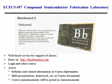
- Web-based service for support of classes.
- Enter at http//blackboard.uc.edu
- Login and select course
- Access
- Syllabus and related information at Course
Information - Slide presentations, homework, etc. at
Course Documents - Course announcements will be posted at
Announcements
2
ECES 697 Compound Semiconductor Fabrication
Laboratory
- Goal To introduce the engineering and
technology of III-V semiconductor device
fabrication, fabrication process design and
device and process characterization. - Prerequisites undergraduate course in
semiconductor materials and devices. - Text None, handouts and copies of
transparencies provided. - Format
- Weekly lecture with handouts
- Weekly lab with GaAs MESFET fabrication project
- Assignments 15
- Lab notebook 20
- Final test 30
- Final project report 35
Source Gate Drain VS 0 VG
lt 0 VD gt 0
-
-
-
-
-
-
-
-
Semi-insulating GaAs substrate
3
Course Overview and Motivation
- Why interest in GaAs MESFETs?
- High speed microwave circuits.
- Simple fabrication process (no epitaxy).
- Low cost.
- Why study the fabrication of GaAs MESFET?
- Introduce device fabrication process
- Simple fab process
- Understand fab process capabilities and
limitations - Complete fab process for MESFET
- Evaluate results of process steps
- Characterize finished devices
- Acquire skills in device fabrication
- Experimental thesis or dissertation work
- Future job
- What are the commercial applications?
4
Submicron Channel GaAs MESFET
Source
Source
Drain
Gate
Gate
Channel width W
Drain
Source
Source
Channel length L
Source
Gate
5
GaAs MESFET Capabilities
- High electron mobility in GaAs channel
gives high drain current ID and
transconductance gm - High electron mobility in GaAs channel
gives short transit time and high speed - Channel transit time
- Cutoff frequency fT
Lg
B. Turner, Ch 10 in GaAs Materials, Devices and
Circuits, Wiley, p. 361 (1985).
6
GaAs MESFET Performance
HEMT
C. W. Tu et al., Ch 4 in GaAs Technology, p. 107
(1985).
7
GaAs MESFET Commercial Applications
- Microwave integrated circuits
- Low noise preamplifiers
- Linear and power amplifiers
- Oscillators and mixers
- Applications
- Satellite communications
- Cellular phones
- Local area networks
- Optoelectronic Integrated Circuits
- Receivers
- Low noise preamplifiers
- Linear amplifiers
- Transmitters
- Laser driver amplifiers
8
Microwave Integrated Circuits
9
Optoelectronic Integrated Circuits
Compound Semiconductor vol. 6 (3), p. 55, April
2000.
10
Course Organization and Overview
- Lecture
- One to two hours weekly (Tuesday)
- Summarize process steps for next stage of device
fab. - What is to done. What is expected. What to be
measured. What calculations and analysis. - Present some theoretical background on processes
- Outline important measurements, calculations and
analysis of results. - Lab
- Four hour lab session weekly (Wednesday or
Thursday) - Initial demonstration of process and equipment
use. - Wafer processing
- Student groups of two or three
- Evaluation of results
- GaAs MESFET Fabrication
- Mask design
- Silicon nitride deposition
- Photolithography
- Mask alignment
- Optical exposure
- Resist development and processing
- Ion implantation
- SiN etching (wet and RIE)
- Metallization
- Ohmic contact
- Schottky contact
- Liftoff process
- Rapid thermal annealing
- MESFET characterization
- Test structure measurements
11
GaAs MESFET Fabrication Process
12
Course Schedule
13
Course Requirements and Grading
- Final Lab Report (35)
- Executive summary of device fab and results
obtained - Prepared by each student group (2 or 3)
- Typewritten, organized, well written
- Overview of fab process
- What was done, what achieved, what expected, what
problems, what results, why - Stand alone, inclusive of all results
- Process measurements and results
- Calculations, graphs and analysis
- Comparison with theoretical calculations and
analysis of differences from measurements - Summary of results, e.g. process successes or
sources of problems, performance of device,
analysis of test structure results.
- Lab Notebook (20)
- Keep notes from fab
- Key equipment settings and notes on operation
- Important observations, measurements,
calculations and analysis - Graded
- Lab Assignments (15)
- Weekly report on lab results
- Organized, neat
- Observations, measurements, example calculations
and analysis of results. - Final Test (30)
- Exam week
- Knowledge of fab process
- Theoretical calculations
- MESFET measurements
- Test structure operation and use
Recommended
