
CCDs for DECam PowerPoint PPT Presentation
1 / 9
Title: CCDs for DECam
1
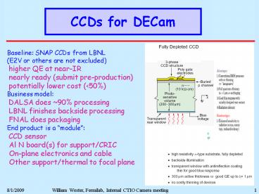
CCDs for DECam
Baseline SNAP CCDs from LBNL (E2V or others are
not excluded) higher QE at near-IR nearly ready
(submit pre-production) potentially lower cost
(processing LBNL finishes backside processing
FNAL does packaging End product is a module
CCD sensor Al N board(s) for support/CRIC
On-plane electronics and cable Other
support/thermal to focal plane
2
Near IR Response
3
Recent progress
- LBNL has received v.1 SNAP wafers
- Business model continues to look promising
- In December, concern was the last top metal step.
Normally Al could not withstand a high
temperature backside process. DALSA top metal
processing with Ti N looks promising - LBNL did acquire a plasma etcher for top side
processing with Al - CRIC prototype has read out a LBNL CCD
- LBNL desires an on-site furnace (400K)
4
SNAP 150mm layout
SNAP 18 mm pixel spectrograph CCD
800 x 1980 NOAO MARS (2x, 1 12 mm pixel with
design for high voltage)
470 x 1264 24mm Lick Guider (2x) (1 with 2-stage
amp)
SNAP 35122
Template for 100 mm cut down if necessary
1k x 512 (4x)
2210 x 802 9mm 2-stage amps (4) 20 fps (4x)
SNAP 9 mm Pixel spectrograph CCD 2226 x 868
5
SNAP 18 mm pixel spectrograph CCD
800 x 1980 NOAO MARS (2x, 1 12 mm pixel with
design for high voltage)
470 x 1264 24mm Lick Guider (2x) (1 with 2-stage
amp)
SNAP 35122
1k x 512 (4x)
2210 x 802 9mm 2-stage amps (4) 20 fps (4x)
SNAP 9 mm Pixel spectrograph CCD 2226 x 868
6
Meeting at LBNL
- Random thoughts of M. Levi, C. Bebek, S. Holland,
H. von der Lippe, W. Wester, and J. Fast - Modification of mask design 1 week effort with
3 months of verification - No specific 2K x 4K submissions
- Readout 100kps could be increased x2
- Packaging is a major issue 50K for packaged
devices seems like a bargain. - Schedule is a driver
- Packaging going on at Lick, Yale Arizona
7
Other new knowledge
- Slew times closer to 30 sec not 10 sec
- 100 kps readout of 24582 (4 amplifiers) is 15 sec
and 200 kps becomes - Gaps in focal plane layout are important
- Need 5 years to ensure 3 exposures
- Fill factor less important than tiling step
- Its the economy stupid (and the schedule)
- We need to be doing things now with no money
- Baseline SNAP CCDs with 24582 15 mm2
- Use existing SNAP devices as our prototype
- Piggyback (and contribute) to packaging RD
- (2K x 4K not completely excluded)
8
Focal plane layout
- Still some options that depend mostly on the
corrector. 70 devices, 74, or 79
420mm FOV
9
Cost and schedules
- Work towards reading out CCDs at FNAL
- 50-100K and 1 year is required
- Buy some SNAP CCDs
- Pay for some packaging
- Set-up dewar
- Set-up test stand
- Production order 1-1.5M
- 48 wafers x 4 devices x 50 yield 96 gradeA
- Includes packaging MS and CRIC chip
- Testing effort 250K (dewars DAQ)
Recommended
