
The STAR Silicon Vertex Tracker PowerPoint PPT Presentation
1 / 54
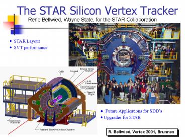
Title: The STAR Silicon Vertex Tracker
1
The STAR Silicon Vertex Tracker
Rene Bellwied, Wayne State, for the STAR
Collaboration
- STAR Layout
- SVT performance
- Future Applications for SDDs
- Upgrades for STAR
R. Bellwied, Vertex 2001, Brunnen
2
RHIC Au-Au Beam Collisions
Approach Collision Particle Shower
R. Bellwied, Vertex 2001, Brunnen
3
Simulated Collision in STAR
Number of tracks in STAR according to a
simulation of a central Au-Au Collision
2000 Central Head-on Peripheral Glancing
R. Bellwied, Vertex 2001, Brunnen
4
Actual Collision in STAR (1)
Actual STAR data for a peripheral collision
5
Actual Collision in STAR (2)
Actual STAR data for a central collision
6
Requirements in a high
multiplicity environment
- General Requirements
- position resolution, two-track resolution
- low radiation length, low cost for large area
- robustness, low integration impact (e.g. cooling,
support) - Specific Requirements
- good energy resolution
- handle high multiplicity environment, reasonable
occupancy - readout speed
R. Bellwied, Vertex 2001, Brunnen
7
The STAR Detector Philosophy
- 1.) We need a reliable technology for standard
tracking (many points, good pattern recognition)
in the high multiplicity environment - chosen technology Time Projection Chamber
- 2.) We need a new technology for vertexing and
low momentum tracking which has to be affordable,
high resolution, and low rad. length - chosen technology Silicon Drift Detectors
R. Bellwied, Vertex 2001, Brunnen
8
The STAR Workhorse The TPC
- Length 4.2 m
- Radial 0.5-2.0 m
- 45 pad rows, 24 sectors
9
STAR-TPC characteristics
- STAR layout
- 45 pad rows (13 in inner sector, 32 in outer
sector) - drift in two directions away from central
membrane - 12 supersectors on each side of the TPC
- resolution 500 mm in r-f-direction, 2 mm in
z-direction - STAR gas
- baseline P-10, Ar (90)-Methane (10), less
hazardous, - more scattering, low max.voltage (31 kV),
- V-gradient 145 V/cm, drift velocity 6cm/ms,
- upgrade He(50)-Ethane(50), better
performance, - higher max.voltage (84 kV)
- Radiation length
- inner field cage 0.62, outer field cage
2.43
R. Bellwied, Vertex 2001, Brunnen
10
The STAR Choice for vertexing
- Silicon Drift Detectors (SDDs)
- assembled in three barrels around beam pipe
- paired with TPC
- detector can vertex and track
- Future applications
- technology suited for very large areas (vs. TPC,
DC, strip) - cheap, robust, easy to integrate, simple
electronics - technology suited for very high resolution (vs.
CCD, APS) - very high resolution at moderate readout pitch
R. Bellwied, Vertex 2001, Brunnen
11
SDDs 3-d measuring devices
R. Bellwied, Vertex 2001, Brunnen
12
The SVT-SDD Characteristics
R. Bellwied, Vertex 2001, Brunnen
13
SDD specific implications
14
Present status of technology
- STAR
- 4in. NTD material, 3 kWcm, 280 mm thick, 6.3 by
6.3 cm area - 250 mm readout pitch, 61,440 pixels per detector
- SINTEF produced 250 good wafers (70 yield)
- ALICE
- 6in. NTD material, 2 kWcm, 280 mm thick, 280 mm
pitch - CANBERRA produced around 100 prototypes, good
yield - Future
- 6in. NTD, 150 micron thick, any pitch between
200-400 mm - 10 by 10 cm wafer
R. Bellwied, Vertex 2001, Brunnen
15
STAR-SVT characteristics
- 216 wafers (bi-directional drift) 432 hybrids
- 3 barrels, 103,680 channels, 13,271,040 pixels
- 6 by 6 cm active area max. 3 cm drift
- 3 mm (inactive) guard area
- max. HV 1500 V
- max. drift time 5 ms, (TPC drift time 50 ms)
- anode pitch 250 mm, cathode pitch 150 mm
- 25 ns time buckets in y-direction
- corresponds to approximately square pixels
- ENC 500 e
- 0.44 m long
R. Bellwied, Vertex 2001, Brunnen
16
Wafers Resolution
R. Bellwied, Vertex 2001, Brunnen
17
Wafers Noise Dynamic Range
- Low capacitance anodes
- only 530e noise.
- (PASA 380e
- SCA 300e
- bond wire 30e)
- Diffusion of electron cloud allows large dynamic
range (50MIP).
R. Bellwied, Vertex 2001, Brunnen
18
Wafers Integrated Charge
- No evidence of charge loss. Large signal at full
drift (simplifies hit finding)
R. Bellwied, Vertex 2001, Brunnen
19
Wafers B and T dependence
- Used at B6T. B fields parallel to drift increase
the resistance and slow the drift velocity. - The detectors work well up to 50oC but are also
very T-dependent. T-variations of 0.10C cause a
10 drift velocity variation - Detectors are operated at room temperature in
STAR. - We monitor these effect via MOS charge injectors
R. Bellwied, Vertex 2001, Brunnen
20
The SVT Multi Chip Module (Hybrid)
R. Bellwied, Vertex 2001, Brunnen
21
The SVT MCM Connections
R. Bellwied, Vertex 2001, Brunnen
22
The SVT FEE Specifications
R. Bellwied, Vertex 2001, Brunnen
23
The SVT Ladder Components
24
Radiation Damage
- Wafer Material High-Res. NTD n-type
- Resistivity 3KW, Inversion at 2 1013/cm2
- FEE bipolar PASA, CMOS-SCA
- PASA rad.hard, SCA rad.soft
- Tests g,n up to 100 krad (1 1012/cm2)
- g causes only surface effects - leakage
current - n causes displacement damage - nonlinearities
- Effects
- S/N degrades from 601 to about 101
- FEE will saturate at about 1 mA/anode
- Reduce resistivity of starting material
- Reduce resistance of implanted resistors
- FEEchange CMOS to rad.hard CMOS
R. Bellwied, Vertex 2001, Brunnen
25
Particle Identification via dE/dx
R. Bellwied, Vertex 2001, Brunnen
26
E896 AGS AuAu (Apr98)
- First tracking device based on Silicon Drift
Detectors. - 15 detectors, 7200 channels, 2 occupancy 60
tracks.ev, - Electronic noise750e, S/N 301
- Operating conditions B6.4T, room temp.
HV operating voltage 1500 V
vdrift 6mm/ns - Dead channels lt1.1 (2 design spec).
- First Successful Measurement of L Polarization in
heavy ion collisions
R. Bellwied, Vertex 2001, Brunnen
27
STAR/SVT at RHIC (BNL)
- Search for the quark-gluon plasma (QGP) and
investigate the behavior of strongly interacting
matter at high energy density. - Installed in February 2001, first beam in July
2001. - 2500 tracks/event in TPC, 40 hits/wafer in SVT
- Radiation length 1.4 per layer
- 0.3 silicon, 0.5 FEE (FrontEnd Electronics),
- 0.6 cooling and support. Beryllium support
structure. - FEE placed beside wafers. Water cooling.
- SVT costs 7M for 0.7m2 of silicon.
R. Bellwied, Vertex 2001, Brunnen
28
The SVT in STAR
Construction in progress
Connecting components
29
The SVT in STAR
The final device.
and all its connections
30
The completed STAR-SVT
Overview while under construction
31
SVT Experiences (I)
- after electronics assembly 99.5 active channels
- after mechanical assembly 97.5 active channels
- after full integration 97 active channels
- loss of channels in mechanical assembly.
Multiplexing in support lines is necessary but
dangerous (e.g. lost 1.5 of channels due to a
single HV line disconnect) - bench resolutions can be reproduced in actual
beam environment - common mode noise is a problem, good shielding is
very important, avoid ground loops - RDO contributes more noise than expected, make
sure that RDO (off-detector) is well shielded as
well
R. Bellwied, Vertex 2001, Brunnen
32
SVT Experiences (II)
- smart zero suppression code very important.
Common mode noise leads to 16 faked occupancy
compared to 2 actual occupancy. Need online
common mode noise subtraction. Part of pedestal
subtraction. Without common mode noise
subtraction the data volume is 4 MByte/ event,
with common mode noise subtraction the data
volume is 0.5 MByte/ event. Raw event size is 20
Mbyte/ event. - when the noise level rises, then the threshold
requirement for zero-suppression leads to small
clusters. Cluster finder has to be optimized for
small cluster (down to single anode clusters).
R. Bellwied, Vertex 2001, Brunnen
33
Silicon Drift Detector Summary
- Mature technology.
- lt10 micron resolution achievable with s and
RD. Easy along one axis (anodes). - lt0.5 radiation length/layer achievable if FEE
moved to edges. - Low number of channels translates to low cost
silicon detectors with good resolution. - Detector could be operated with air cooling at
room temperature - Technology is viable for a vertex detector (very
high position resolution for a small area
detector) or a tracking detector (good resolution
over a large area)
R. Bellwied, Vertex 2001, Brunnen
34
RD for LC Applications
- Improve position resolution to 5mm
- Decrease anode pitch from 250 to 100mm.
- Stiffen resistor chain and drift faster.
- Improve radiation length
- Reduce wafer thickness from 300mm to 150mm
- Move FEE to edges or change from hybrid to SVX
- Air cooling vs. water cooling
- Use 6in instead of 4in Silicon wafers to reduce
channels. - More extensive radiation damage studies.
- Detectors/FEE can withstand around 100 krad (g,n)
- PASA is BIPOLAR (intrinsically rad. hard.)
- SCA can be produced in rad. hard process.
R. Bellwied, Vertex 2001, Brunnen
35
Proposal for LC Detector
- A Six Layer Silicon Drift Tracker (SDT) with max.
cos Q 0.91 in B 5T field - (small detector as alternative to TPC or DC)
- Configuration
- Five layers at radii 20, 46, 72, 99, 125 cm.
- Lengths 53,123,193, 263, 333 cm 56 m2 Silicon
- Wafer size 10 by 10 cm, of Wafers 6000 (incl.
spares) - of Channels 4,404,480 channels (260 mm pitch)
- Issues FEE Integration, Cooling, Support
Structure - different wafer size and thickness in each
- layer to improve radiation length ?
R. Bellwied, Vertex 2001, Brunnen
36
Motivation for a STAR upgrade
- Build Inner tracker (inside SVT) to measure
impact parameter with minimum resolution - Measure D mesons, charm quark production
- Emphasized in the long range plan for STAR
- Window to early hot parton phase
- Large mass, c quarks less less likely from later
mixed phase and hadron phase - More restrictive than measure of strange quark
production - Augments measurements of multi-strange particles,
?- - Calibration of J/? suppression
R. Bellwied, Vertex 2001, Brunnen
37
Technical Challenge of D mesons
- Topological separation of D vertex from primary
vertex with thousands of tracks - D?K-? ? 8 c? 320 ?m
- D0 ? K- ? 3.65 c? 125.9 ?m
- Require microscopic vertex resolution
- minimum coulomb scattering
- Minimum distance to interaction to improve
pointing resolution - Therefore need excellent two track resolution
- excellent position resolution
R. Bellwied, Vertex 2001, Brunnen
38
CCD - VXD3 at SLACa model for our approach
- Very thin, 0.4 radiation length
- High resolution
- pixels - 20 ?m cubes
- surface resolution lt 4 ?m
- projected impact parameter resolution 11 ?m
- Close to beam, inner layer at 2.8 cm radius
- 307 million pixels, lt 1 cent/pixel
R. Bellwied, Vertex 2001, Brunnen
39
VXD3 almost the solution
- Limitations
- Slow readout 200 ms
- Radiation hardness may be a problem in the RHIC
environment. 2 kRad per year - Investigating use of thinned Active Pixel Sensors
(APS) in CMOS in place of CCDs - CMOS design freedom should allow faster readout
solution - APS will have better radiation hardness since
unlike CCDs does not need long charge transport
path through silicon.
R. Bellwied, Vertex 2001, Brunnen
40
Active Pixel Sensor (APS)
- 20 ?m square pixels
- 5 chips per slat
- 90 million pixels
- 40 ?m thick chips
- 760 ?m Be beam pipe
5.6 cm
8 cm
41
RD effort for APS in CMOS
- Can be thinned like CCDs
- Better radiation hardness (TSMC 0.25 ?m CMOS is
good to 40 MRad) - Potentially faster readout and lower power since
zero suppression can be done on the detector chip - Design freedom with standard industry process
- LEPSI demonstrated technology with minimum
ionizing particles - No CMOS APS detectors operating in an experiment
- MIP detection depends on a feature of the CMOS
process that could disappear
R. Bellwied, Vertex 2001, Brunnen
42
Electronics RD plan
- Copy LEPSI style APS
- Using what is learned from the copy investigate
possible readout schemes for power and speed - Possible directions full fast data read vs on
chip zero suppression
Next a look at the LEPSI MIMOSA APS design
R. Bellwied, Vertex 2001, Brunnen
43
A Monolithic Active Pixel Sensor for Charged
Particle Tracking and Imaging using Standard VLSI
CMOS Technology J.D. Berst et al.LEPSI,
Strasbourg
- LEPSI APS
- 20 ?m square pixels
- 64X64 array
- MIMOSA 1, 0.6 ?m CMOS
- MIMOSA 2, 0.35 ?m CMOS
R. Bellwied, Vertex 2001, Brunnen
44
Properties
45
Mechanical Possibilities beyond VXD3 ?
VXD3 Ladder
R. Bellwied, Vertex 2001, Brunnen
46
Conclusion for APS Tracker
- New challenging technology with unknowns
- Significant potential gains
- Important for STAR Long Range Plan
- Could benefit other RHIC experiments and heavy
ion program at LHC - Cost 3-4 M
- Time 3-4 years
R. Bellwied, Vertex 2001, Brunnen
47
Performance
R. Bellwied, Snowmass 2001
48
First chip submission
S. Kleinfelder
49
MIMOSA Readout and noise reduction
- Read out all pixels, 12 bit ADC
- MIMOSA I at 2.5 MHz
- MIMOSA II at 10 MHz
- Correlated Double Sample (CDS) offline to remove
Reset thermal (kTC) and Fixed Pattern noise - Average baseline subtraction to remove leakage
current pedestal
R. Bellwied, Snowmass 2001
50
Readout options depend on chip performance
- If the following noise sources are low compared
to the signal then simple threshold zero
suppression can be used - reset kTC noise (thermal)
- reset fixed pattern noise
- diode leakage current
- Expected MIP signal 640 e
- Expected reset kTC noise 30 to 40
- Expected reset fixed pattern ?
- Diode leakage current 0.25 fA to 29 fA
R. Bellwied, Snowmass 2001
51
APS Readout with Zero Suppression if noise permits
- Readout of each row followed by threshold
discrimination and zero suppression in columns. - No additional logic in pixels.
- Minimal periphery in one dimension allows close
abutting.
S. Kleinfelder
52
Zero suppression if only reset fixed pattern
noise is a problem
- When a trigger occurs a CDS is done with a reset
between samples. This removes reset fixed
pattern noise, but not reset kTC noise. - Reset is done one row at a time. Could have a
separate readout on each column.
R. Bellwied, Snowmass 2001
53
Zero suppression if large pixel to pixel
variation and large reset noise (the heroic
solution)
- Full independent CDS on each pixel before doing
threshold check - Do by continuous digitization and store into on
chip dynamic RAM in a few ms for all pixels - On trigger digitize and subtract memory value to
obtain CDS for threshold check - Dynamic RAM only 1/10 pixel area
- Need power analysis, but experience suggests 100
mW/cm2 limit possible
R. Bellwied, Snowmass 2001
54
Alternative readout mode
- Full pixel readout - continuous
- 20 40 ms per read (slower than other detector
readouts) - Off chip correlated double sampling
- Chip design may be simpler, but enhancements
required like column parallel operations etc. - Complicated DAQ and data processing
- Filled pixels still lt 3 at 10 X design
luminosity - Should be able to stay in 100 mW/cm2 power budget
R. Bellwied, Snowmass 2001
Recommended
