
MOSFET CrossSection PowerPoint PPT Presentation
1 / 56
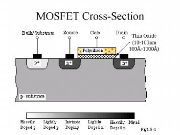
Title: MOSFET CrossSection
1
MOSFET Cross-Section
2
A MOSFET Transistor
Source
Drain
Gate
Drain
Gate
Source
Substrate
3
MOSFET Schematic Symbols
4
Formation of the Channel for an Enhancement MOS
Transistor
5
Water Analogy of a (subthreshold) MOSFET
6
Channel Current vs. Gate Voltage
Above-Threshold
Sub-Threshold
450
-3
10
400
-4
10
In linear scale, we have a quadratic dependence
-5
350
10
300
-6
10
250
-7
In log-scale, we have an exponential dependence
Channel Current (mA)
10
Channel Current (A)
200
-8
10
150
-9
10
100
-10
10
50
-11
10
0
-12
10
0
0.5
1
1.5
2
2.5
3
3.5
4
4.5
5
0.4
0.6
0.8
1
1.2
1.4
1.6
1.8
2
Gate voltage (V)
Gate voltage (V)
7
MOS Capacitor Picture
8
MOSFET Channel Picture
9
MOS Capacitor Picture
10
MOS Electrostatics
Vfb
Condition is called flatband --- the voltage when
this occurs is called flatband
This state is the baseline operating case --- a
capacitive divider has one free parameter
11
MOS Electrostatics
Depletion Condition --- gate charge is terminated
by charged ions in the depletion region
Part of this region is often referred to as
weak-inversion
12
MOS Electrostatics
Inversion --- further gate charge is terminated
by carriers at the silicon--silicon-dioxi
de interface
13
MOS Structure Electrostatics
14
MOS Capacitor Picture
15
MOS-Capacitor Regions
16
MOS Capacitor Picture
17
MOSFET Channel Picture
18
Calculation of Drain Current
19
2
n
d
No recombination
Dn Ax B
0
Dn
0
0
2
dx
0
D
2
n
d
dn
-
R
G
D
n
2
dx
dt
0
l
y varies as kVG
(
)
(
)
(
)
-
-
k
k
U
V
V
U
V
V
/
/
-
e
e
I
I
T
d
g
T
S
g
0
20
MOSFET Current-Voltage Curves
(
)
-
-
/
/
/
u
V
u
V
u
kV
-
e
e
e
I
I
T
D
T
S
T
G
0
DS
(
)
(
)
(
)
-
k
/
u
V
V
-
-
-
/
u
V
V
1
e
e
I
T
S
g
T
S
d
0
(
)
-
-
/
/
)
(
u
V
u
V
kV
-
1
e
e
I
T
ds
T
S
G
0
gt
4
U
V
-
/
)
(
u
V
kV
e
I
T
ds
T
S
G
0
Saturation
21
MOSFET Current-Voltage Curves
(
)
-
-
/
/
/
u
V
u
V
u
KV
-
e
e
e
I
I
T
D
T
S
T
G
0
DS
(
)
(
)
(
)
-
k
/
u
V
V
-
-
-
/
u
V
V
1
e
e
I
T
S
g
T
S
d
0
(
)
-
-
/
/
)
(
u
V
u
V
KV
-
1
e
e
I
T
dS
T
S
G
0
-
/
)
(
u
V
KV
e
I
T
S
G
0
22
Subthreshold MOSFETs
In linear scale, we have a quadratic dependence
In log-scale, we have an exponential dependence
23
Determination of Threshold Voltage
24
Drain Current --- Source Voltage
25
Drain Characteristics
26
Origin of Drain Dependencies
Increasing Vd effects the drain-to-channel
region
- increases barrier
- height
- increases depletion
- width
27
Current versus Drain Voltage
Not flat due to Early effect (channel length
modulation)
Id Id(sat) (1 (Vd/VA) ) or Id Id(sat)
eVd/VA
28
Early Voltage Length Dependence
Width of depletion region depends on doping, not L
Might expect Vo to linearly vary with L
29
MOSFET Operating Regions
Surface potential moving from depletion to
inversion
Band-diagram picture moving from subthreshold
to above-threshold
30
Qualitative Above-Threshold
I (K/2k) (( k(Vg - VT) - Vs )2 - (( k(Vg - VT)
- Vd )2 )
31
Above Threshold MOSFET Equations
I (K/2k) ( (k(Vg - VT) - Vs)2
- (k(Vg - VT ) - Vd) 2 )
If k 1 (ignoring back-gate effects)
I (K/2) ( 2(Vgs - VT) Vds - Vds2 )
Saturation Qd 0
I (K/2k) ( (k(Vg - VT) - Vs)2
32
Detailed MOSFET Derivation
Q(x) CT ( k(Vg - VT) - V(x))
CT CD Cox
Qs CT ( k(Vg - VT) - Vs), Qd CT ( k(Vg -
VT) - Vd)
(k Cox / CT)
Current is constant through the channel (no
loss)
I m Q(x) E(x)
( E(x) Electric Field )
33
Detailed MOSFET Derivation
d Q(x) dx
Integrate with respect to length I (m / CT )
Q(x)
I (m / 2 CT ) ( 1 / L) (Qs2 - Qd2)
I (m CT / 2 ) ( 1 / L) (( k(Vg - VT) - Vs) 2 -
( k(Vg - VT) - Vd)2)
K m Cox (W/L)
I (K/2k) (( k(Vg - VT) - Vs )2 - (( k(Vg - VT)
- Vd )2 )
34
MOSFET Equations
When ignoring back-gate effects (we often
do) k 1
I (K/2) ( (Vg - VT - Vs)2 - (Vg - VT - Vd) 2 )
Above-Threshold
I (K/2) ( 2(Vgs - VT) Vds - Vds2 )
Saturation (Qd 0)
I (K/2) (Vgs - VT )2
(Vd gt Vg - VT )
-Vds/UT
Vgs/UT
I Is e (1 e )
Subthreshold
Vgs/UT
Saturation (Vdsgt 4 UT) I Is e
35
Output Characteristics of the Above-Threshold
MOSFET
Interpretation of large-signal model
36
MOSFETs
K 37.861 mA/V2
VT 0.806
37
Drain Current - Gate Voltage
38
Drain Current --- Source Voltage
4
3.5
K/k 74.585 mA/V2
3
(k 0.7)
2.5
sqrt(Drain current (mA))
2
1.5
k (Vg - VT) 0.595
1
(k 0.54)
0.5
0
0
0.1
0.2
0.3
0.4
0.5
0.6
0.7
0.8
0.9
1
Gate voltage (V)
39
An Ohmic MOSFET
I (K/2k) ( (k(Vg - VT) - Vs)2 -
(k(Vg - VT ) - Vd) 2 )
If Vd Vs, (small difference)
I K (Vg - VT)(Vd - Vs)
40
A MOSFET in Saturation
Saturation Qd 0
I (K/2k) ( (k(Vg - VT) - Vs)2
41
More Ohmic Region Data
I (K/2k) ( (k(Vg - VT) - Vs)2 -
(k(Vg - VT ) - Vd) 2 )
Take the derivative of I with respect to Vd
(Vs 0 )
dI / d Vd (K/2k)( 0 - (-2) (k(Vg - VT
) - Vd) ) (K/2k)(k(Vg - VT ) - Vd)
42
Influence of VDS on the Output Characteristics
43
Current versus Drain Voltage
Not flat due to Early effect (channel length
modulation)
Id Id(sat) (1 (Vd/VA) ) or Id Id(sat)
eVd/VA
44
Early Voltage Length Dependence
Width of depletion region depends on doping, not L
Might expect Vo to linearly vary with L
45
Small-Signal Modeling
V3
V -
V1
V3
V2
I
I
gmV
ro
V1
V1
V3
V2
V2
V2
gm
ro
Av
Above VT MOSFET
2I /(V1-V2 -VT)
VA / I
2VA/(V1-V2 -VT)
Sub VT MOSFET
I / UT
VA / I
VA / UT
46
Small-Signal Modeling
V3
V3
I
I
V1
V1
V2
V2
gm
ro
rp
Av
BJT
(UT b) / I
I / UT
VA / I
VA / UT
Above VT MOSFET
2I /(V1-V2 -VT)
VA / I
2VA/(V1-V2 -VT)
?
Sub VT MOSFET
?
I / UT
VA / I
VA / UT
47
Capacitances in a MOSFET
48
MOSFET Depletion Capacitors
49
Overlap Capacitances
50
Capacitance Modeling
51
Capacitance Modeling
52
Velocity Saturation
53
Effect of Velocity Saturation
Square-law region
VT
L 76 nm MOSFET
54
(No Transcript)
55
Small-Signal Modeling (with kappa)
V3
V -
V1
V3
V2
I
I
gmV
ro
V1
V1
V3
V2
V2
V2
gm
ro
Av
Above VT MOSFET
2I /(V1-V2 -VT)
VA / I
2VA/(V1-V2 -VT)
Sub VT MOSFET
kI / UT
VA / I
kVA / UT
56
Small-Signal Modeling (with kappa)
V3
V3
I
I
V1
V1
V2
V2
gm
ro
rp
Av
BJT
(UT b) / I
I / UT
VA / I
VA / UT
Above VT MOSFET
2I /(V1-V2 -VT)
VA / I
2VA/(V1-V2 -VT)
?
Sub VT MOSFET
kI / UT
?
VA / I
kVA / UT
Recommended
