Complete OCR Schematic PowerPoint PPT Presentation
Title: Complete OCR Schematic
1
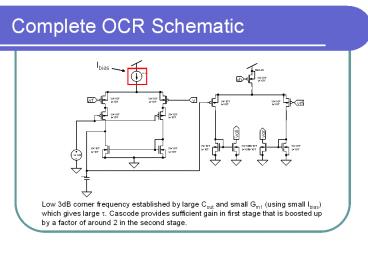
Complete OCR Schematic
Ibias
Low 3dB corner frequency established by large
Cout and small Gm1 (using small Ibias) which
gives large t. Cascode provides sufficient gain
in first stage that is boosted up by a factor of
around 2 in the second stage.
2
Circuit Block Diagram
The DC gain of the offset correction circuit is
set by Gm1Ro and the corner frequency is set by
Gm1Cout. Gm2 is the V-to-I conversion to allow a
current feedback into the original filter OTA.
3
AC Response Verification
Q2 f90300Hz Q2
f902kHz
4
Stability Verification
5
DC Behavior and Startup Time
DC behavior of OCR Startup
time verification
6
Final Results
- Q2, f9010kHz filter uses 6.13mW (bonus)
- f90 variable from 100Hz to 10kHz Q variable from
1 to 6 - Effective noise sources N4.81, VL0.765V which
results in DR gt 60dB - Filter attenuation at HF past f90 -75dB lt 1dB
variation from unity gain in passband - Power to correct 10kHz filter 480.48nW
- Power-on startup time 0.12s (bonus)
- 14 transistors used for OCR circuit (bonus)
- Maximum cap size 10pF
- Lowest current used 0.16nA
- Entire layout fits in ¼ of padring area (bonus)
7
Full Chip Layout
PowerShow.com is a leading presentation sharing website. It has millions of presentations already uploaded and available with 1,000s more being uploaded by its users every day. Whatever your area of interest, here you’ll be able to find and view presentations you’ll love and possibly download. And, best of all, it is completely free and easy to use.
You might even have a presentation you’d like to share with others. If so, just upload it to PowerShow.com. We’ll convert it to an HTML5 slideshow that includes all the media types you’ve already added: audio, video, music, pictures, animations and transition effects. Then you can share it with your target audience as well as PowerShow.com’s millions of monthly visitors. And, again, it’s all free.
About the Developers
PowerShow.com is brought to you by CrystalGraphics, the award-winning developer and market-leading publisher of rich-media enhancement products for presentations. Our product offerings include millions of PowerPoint templates, diagrams, animated 3D characters and more.

