
Design Flow Overview PowerPoint PPT Presentation
1 / 5
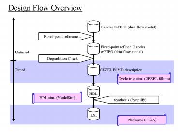
Title: Design Flow Overview
1
Design Flow Overview
C codes w/FIFO (data-flow model)
Fixed-point refinement
Fixed-point refined C codes w/FIFO (data-flow
model)
Untimed
Degradation Check
GEZEL FSMD description
Timed
Cycle-true sim. (GEZEL fdlsim)
HDL
HDL sim. (ModelSim)
Synthesis (Synplify)
LSI
Platforms (FPGA)
2
Implementation of H/W JPEG Encoder
- Design rules and constraints
- Design policy single clock usage positive
edge-triggered synchronous design - Input language GEZEL
- System clock frequency 60MHz clock
- Performance Requirement enable to encode UXGA
size (1600 x 1200 pixels) of RGB888 data _at_ 15fps
(frames / sec). - gt How many cycles could be used for
computing each function? Which one has the worst
number? - Target system architecture
- Pipeline in system-level and functional-block-leve
l - Use single-port SRAM for b1, b2, b3, b4, b5.
- Use double buffering of the SRAMs for
communication between functional blocks (for
simplicity to escape any ram access conflicts)
3
Block Diagram for JPEG Encoder
Max. rate UXGA_at_15fps
JPEG Encoder
b5
RGB
b1
b2
b3
rgbyuv
dct
camif
Trgbyuv
Tdct
Tcamif
Main FSM
b4
b6
quant
huf
fdump
Tquant
Thuf
b3
JPEG
RAM
BLOCK
Txxx Number of cycle needed for block xxx
4
Schedule for each block of JPEG Encoder(1)
- System-level Pipelining buffer access
Access conflict occurred with b2
b4 Read
b4 Read
b4 Read
b4 Write
b4 Write
b4 Write
b4 Write
b3 Read
b3 Read
b3 Read
b3 Read
b3 Write
b3 Write
b3 Write
b3 Write
b3 Write
b2 Read
b2 Read
b2 Read
b2 Read
b2 Read
b2 Write
b2 Write
b2 Write
b2 Write
b2 Write
b2 Write
time
rgbyuv
rgbyuv
rgbyuv
rgbyuv
rgbyuv
rgbyuv
dct
dct
dct
dct
dct
..
quant
quant
quant
quant
huf
huf
huf
Tworst (in this figure DCT has the worst of
cycles)
5
Schedule for each block of JPEG Encoder(2)
- Input image data is stored in b1 line by line
(raster-scan) on-the-fly.- 1 pixel of R,G,B is
assumed to be input at every two cycles _at_60MHz
(speed of UXGA_at_15fps)- On the other hand, jpeg
deals with 8 x 8 blocks gt Encoding can start
when 8 lines are all stored in b1.- The below
shows a scheduling example of the JPEG encoder
for 64 x 64 pixels
START
RGB Input (camif)
1st 8lines
2nd 8lines
3rd 8lines
RGBYUV
1
2
3
4
5
6
7
8
DCT
..
2
1
3
5
4
6
7
Quant
1
2
3
4
5
6
HUFF
1
2
3
4
5
RGB Input
8th 8lines
RGBYUV
57
58
59
60
61
62
63
64
..
DCT
64
57
56
58
59
61
60
62
63
Quant
64
64
55
56
57
58
59
60
61
62
HUFF
62
63
64
54
55
56
57
58
59
60
61
END
Recommended
