
CMOS 60GHz Beamforming Circuit Design for Active Imaging Application - PowerPoint PPT Presentation
1 / 1
Title:
CMOS 60GHz Beamforming Circuit Design for Active Imaging Application
Description:
CMOS 60GHz Beamforming Circuit Design for Active Imaging Application Saihua Lin, Ada Poon, Simon Wong saihua_at_stanford.edu, adapoon_at_stanford.edu, wong_at_stanford.edu – PowerPoint PPT presentation
Number of Views:43
Avg rating:3.0/5.0
Title: CMOS 60GHz Beamforming Circuit Design for Active Imaging Application
1
CMOS 60GHz Beamforming Circuit Design for Active
Imaging Application
Saihua Lin, Ada Poon, Simon Wong
saihua_at_stanford.edu, adapoon_at_stanford.edu,
wong_at_stanford.edu
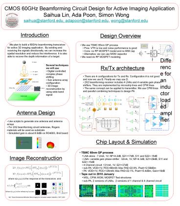
Introduction
Design Overview
We plan to build a 60GHz beamforming
transceiver for active 3D imaging application.
By sending and receiving the signals
directionally, we can increase the spatial
resolution and reduce the interference. It is
also able to recover the depth information of a
target.
- We use TSMC 65nm GP process
- Pros VTH is low and noise performance is good
- Cons no RF MOSFET model and no MIM cap
- Alternative we can use MOM capacitor
- We need do RF MOSFET modeling
Difference for an inductor loaded amplifier
- Several techniques we will use
- Digital controlled complex phase shifting
- Sub antenna array configuration
- 3D image reconstruction by using wide band signal
Rx/Tx architecture
- There are 4 configurations for Tx and Rx.
Configuration A is not good and now we use B.
Finally we may use D. - 2X2 beamforming receiver includes 4 LNAs and 4
variable gain phase shifters. They are
implemented by microstrip lines and CPW lines - The same concept can be applied to transmitter.
We use CPW lines and parallel combining
techniques to design PA
Antenna Design
- Use scripts to generate one antenna and antenna
arrays - For 2X2 beamforming cirucit antennas, Rogers
materials will be used as substrate - Simulated gain is about 6.9dBi on RO4003, 8mil
board
Chip Layout Simulation
- TSMC 65nm GP process
- LNA alone 7.2mA, 1V, NF4.2dB, S2117dB, S11
and S22lt-15dB - LNA variable gain phase shifter 32mA, 1V,
NF4.3dB, S2129dB, S11 and S22lt-15dB - 4 Channel circuit 131mA, 1V, S2137dB
- sub-PA VDD1V, PDC66mW, Max PAE22.9,
Psat12.58dBm - PA VDD1V, PDC128mW, Max PAE22.1,
Psat15.4dBm, Gain19dB - Tape out in 2010 January
- MSL, CPW, MOM, MOSFET Test structures
- sub-PA, 2 versions of LNAs, 2 versions of 1
channel 4 channel circuit
Image Reconstruction
where s(x,y,?) is the response at the
transceiver, and
Where f(x,y,z) is the reflectivity function
2D FFT
3D FFT
Ref Three-Dimensional Millimeter-Wave imaging
for concealed weapon detection, TMTT 2001
Recommended
CrystalGraphics Presentations


