
Data Acquisition ET 228 Chapter 15 - PowerPoint PPT Presentation
Title:
Data Acquisition ET 228 Chapter 15
Description:
Data Acquisition ET 228 Chapter 15 Subjects Covered Analog to Digital Converter Characteristics Integrating ADCs Successive Approximation ADCs Flash ADCs – PowerPoint PPT presentation
Number of Views:192
Avg rating:3.0/5.0
Title: Data Acquisition ET 228 Chapter 15
1
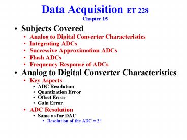
Data Acquisition ET 228Chapter 15
- Subjects Covered
- Analog to Digital Converter Characteristics
- Integrating ADCs
- Successive Approximation ADCs
- Flash ADCs
- Frequency Response of ADCs
- Analog to Digital Converter Characteristics
- Key Aspects
- ADC Resolution
- Quantization Error
- Offset Error
- Gain Error
- ADC Resolution
- Same as for DAC
- Resolution of the ADC 2n
2
Data Acquisition ET 228Chapter 15
- Analog to Digital Converter Characteristics
- ADC Resolution
- Same as for DAC
- Text commonly uses 1 LSB for ?Vin for a change of
1 LSB - Text commonly uses FSR for VFSR
- Maximum Identifiable Input Voltage
- Text commonly refers to it as Vifs and calls it
the Maximum Full Scale Input Voltage - Vifs FSR - 1 LSB
- Causes all ones in the binary output
- Digital Output
- D VIN/1 LSB
- Input/Output Graph for an ideal 3-bit ADC
- Figure 15-1 on page 432
- Sample Problem
- 15-1 on page 432
3
Data Acquisition ET 228Chapter 15
- Analog to Digital Converter Characteristics
- ADC Resolution
- In Class Exercise
- Problem 1 on page 451 w/ 2.4V, 3.0V, and 4.5V as
the input voltages - Quantization Error
- Review Figure 15-1 for a Digital Output of 1/2
FSR or D1002 - Output is the same for the Inputs 1/2 LSB
around the center - This uncertainty is the quantization error
- Offset Error
- Output is off from the Ideal
- Usually expressed in terms of the LSB
- See Figure 15-2 on page 433
- Example Problem 15-2 on page 434
- In class exercise Example 15-2 but for Offset
Error of 1/2 LSB
4
Data Acquisition ET 228 Chapter 15
- Analog to Digital Converter Characteristics
- Gain Error
- Usually specified as a percentage of FSR
- A positive Gain Error lowers the input V that
will yield all 1s - See Figure 15-3 on page 434
- Example Problem 15-3 on page 435
- Linearity Error
- Figure 15-4 on page 435
- Types of ADCs
- Integrating
- Usually for slowly changing Analog Inputs
- Usually needs approximately 300 ms
- Successive Approximation
- Converges in a few microseconds
5
Data Acquisition ET 228Chapter 15
- Types of ADCs
- Flash Converters
- More costly
- Much faster - can be used to digitize video
signals - Integrating ADCs
- Key Phases of the conversion
- Signal Integrate
- Reference Integrate
- Auto-Zero
- See Figure 15-5 on page 437
- Signal Integrate Phase
- Input Analog signal is applied to the Integrator
- Must be in the FSR of inputs
- Vo ramps up in the opposite polarity of the input
6
Data Acquisition ET 228Chapter 15
- Integrating ADCs
- Signal Integrate Phase
- Sample
- Vin -100 mV ----Vout of 833mV
- The Counter went through 1000 counts - each
lasting 83.3?s for a total of 83.3 ms - Period T1
- Reference Integrate
- During T1 a capacitor Cref was charged with the
reference voltage - Constant magnitude, but with the opposite
polarity of Vin - The higher Vin the longer this period of time T2
- See Figure 15-5 the T2 for Vin -200 mV is
twice the period for Vin -100 mV - T2 (Vin/Vref) T1
- with Vref 100 mV T1 83.3 ms
- T2 (0.833 ms/mV)Vin
7
Data Acquisition ET 228Chapter 15
- Integrating ADCs
- Reference Integrate
- The Conversion
- Digital Output (counts/second) T2
- (counts/second) T1 (Vin/Vref)
- with Vref 100 mV T1 83.3 ms
- Digital Output 12,000 (counts/second) (83.3
ms/100 mV) Vin - with Vref 100 mV T1 83.3 ms
- (10 counts/mV) Vin
- Sample Problem 15-5 on page 439.
- The Auto-Zero
- Cint is zeroed out
8
Data Acquisition ET 228Chapter 15
- Successive Approximation ADCs
- Uses a DAC and is digitally controlled
- See Figure 15-6 on page 440
- Key Components
- Comparator
- DAC
- Successive Approximation Register (SAR)
- Eternal Logic Circuits
- Process
- DAC generates a signal that is compared with the
input - Only Greater Than or Less Than Comparisons
- Number of comparisons equal to the number of bits
- much less than the number of possible DAC
output values - 3 bit gt 3 verses 8 tests
- 8 bit gt 8 verses 256 tests
9
Data Acquisition ET 228Chapter 15
- Successive Approximation ADCs
- Process
- Walk through Figure 15-7 on page 441
- Note timing error with the Start and clock pulses
- Conversion Time
- Each of the comparisons uses a clock cycle
- Assumption the circuits are reset before the
start of the test - The resetting requires at least one clock cycle
- ? TC T(n 1)
- T period of the clock pulse
- n the number of bits in the resolution of the
ADC - the period of time required to perform a
Successive Approximation A/D conversion - Example Problem 15-6 on page 442
10
Data Acquisition ET 228Chapter 15
- Flash ADCs
- Very Component Intensive
- A 3-bit Flash ADC
- At least seven Comparators
- Eight to 3 line converter
- Each input line causes a specific pattern on the
three line output - A 8-bit Flash ADC
- At least 255 Comparators
- 256 to eight line converter
- Each input line causes a specific pattern on the
eight line output - A 10-bit Flash ADC
- At least 1023 Comparators
- 1024 to ten line converter
- Conversion Time
- Only limited by the response times of the
- Comparators
11
Data Acquisition ET 228Chapter 15
- Flash ADCs
- Conversion Time
- Only limited by the response times of the
- Logic Gates in the line converter
- Number of comparators
- 2n - 1
- Frequency Response of ADCs
- Key Aspects
- Aperture Error
- Sample-and-Hold Amplifiers
- Aperture Error
- Caused by Input changing more than 1/2 LSB
- Formula for the upper frequency limit for
accurate A/D conversion of a sine wave
12
Data Acquisition ET 228Chapter 15
- Frequency Response of ADCs
- Aperture Error
- Example Problem 15-7 on page 450
- ADC 8-bit w/TC 10 µsec
- v Asin?t Asin(2pf)t
- Simplifying assumptions A 1V
- ?T 10 µsec
- fMax 62Hz, 1 LSB 2V/256 7.8125 mV, 0.5LSB
3.906mV - v Asin(2pf)t w/t0 µsec, and f 61 Hz
- v sin (6.2831853 61) 0 0
- Asin(2pf)t w/t10 µsec, and f 61 Hz
- v sin (6.2831853 61) 10 µsec 3.833mV
- v Asin(2pf)t w/t0 µsec, and f 63 Hz
- v sin (6.2831853 63) 0 0
- Asin(2pf)t w/t10 µsec, and f 63 Hz
- v sin (6.2831853 63) 10 µsec 3.958mV
13
Data Acquisition ET 228Chapter 15
- Frequency Response of ADCs
- Sample-and-Hold Amplifier
- Key to increasing the Frequency response of ADCs
- Two OP-Amp Circuit with a high speed switch
- Figure 15-13 on page 451
- Takes inputs when the switch is closed
- The Cap holds the inputted signal constant while
it is converted by an external ADC - ? The TC can be used to represent the switch
jitter variation - Usually a much smaller number than the ADC
conversion time - Sample Problem 15-8 on page 451
Recommended
CrystalGraphics Presentations


