
Activity 2 : Use of CCD Cameras. - PowerPoint PPT Presentation
Title:
Activity 2 : Use of CCD Cameras.
Description:
Applying low quality flat fields and bias frames to scientific data ... Averaging 5 frames will reduce the amount of read noise (electronic noise from the CCD ... – PowerPoint PPT presentation
Number of Views:68
Avg rating:3.0/5.0
Title: Activity 2 : Use of CCD Cameras.
1
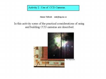
Activity 2 Use of CCD Cameras.
Simon Tulloch smt_at_ing.iac.es
In this activity some of the practical
considerations of using and building CCD cameras
are described.
Nik Szymanek
2
Spectral Sensitivity of CCDs
The graph below shows the transmission of the
atmosphere when looking at objects at the
zenith. The atmosphere absorbs strongly below
about 330nm, in the near ultraviolet part of the
spectrum. An ideal CCD should have a good
sensitivity from 330nm to approximately 1000nm,
at which point silicon, from which CCDs are
manufactured, becomes transparent and therefore
insensitive.
Over the last 25 years of development, the
sensitivity of CCDs has improved enormously, to
the point where almost all of the incident
photons across the visible spectrum are detected.
CCD sensitivity has been improved using two main
techniques thinning and the use of
anti-reflection coatings. These are now
explained in more detail.
3
Thick Front-side Illuminated CCD
Incoming photons
p-type silicon
n-type silicon
Silicon dioxide insulating layer
625mm
Polysilicon electrodes
These are cheap to produce using conventional
wafer fabrication techniques. They are used in
consumer imaging applications. Even though not
all the photons are detected, these devices are
still more sensitive than photographic
film. They have a low Quantum Efficiency due to
the reflection and absorption of light in the
surface electrodes. Very poor blue response. The
electrode structure prevents the use of an
Anti-reflective coating that would otherwise
boost performance. The amateur astronomer on a
limited budget might consider using thick CCDs.
For professional observatories, the economies of
running a large facility demand that the
detectors be as sensitive as possible thick
front-side illuminated chips are seldom if ever
used.
4
Anti-Reflection Coatings 1
Silicon has a very high Refractive Index (denoted
by n). This means that photons are strongly
reflected from its surface.
2
ni
Fraction of photons reflected at the interface
between two mediums of differing refractive
indices
nt
n of air or vacuum is 1.0, glass is 1.46, water
is 1.33, Silicon is 3.6. Using the above equation
we can show that window glass in air reflects
3.5 and silicon in air reflects 32. Unless we
take steps to eliminate this reflected portion,
then a silicon CCD will at best only detect 2 out
of every 3 photons. The solution is to deposit a
thin layer of a transparent dielectric material
on the surface of the CCD. The refractive index
of this material should be between that of
silicon and air, and it should have an optical
thickness 1/4 wavelength of light. The
question now is what wavelength should we choose,
since we are interested in a wide range of
colours. Typically 550nm is chosen, which is
close to the middle of the optical spectrum.
5
Anti-Reflection Coatings 2
With an Anti-reflective coating we now have three
mediums to consider
ni
Air
ns
AR Coating
nt
Silicon
The reflected portion is now reduced to In
the case where the
reflectivity actually falls to zero! For silicon
we require a material with n 1.9, fortunately
such a material exists, it is Hafnium Dioxide. It
is regularly used to coat astronomical CCDs.
6
Anti-Reflection Coatings 3
The graph below shows the reflectivity of an EEV
42-80 CCD. These thinned CCDs were designed for
a maximum blue response and it has an
anti-reflective coating optimised to work at
400nm. At this wavelength the reflectivity falls
to approximately 1.
7
Thinned Back-side Illuminated CCD
Anti-reflective (AR) coating
Incoming photons
p-type silicon
n-type silicon
Silicon dioxide insulating layer
Polysilicon electrodes
The silicon is chemically etched and polished
down to a thickness of about 15microns. Light
enters from the rear and so the electrodes do
not obstruct the photons. The QE can approach
100 . These are very expensive to produce since
the thinning is a non-standard process that
reduces the chip yield. These thinned CCDs
become transparent to near infra-red light and
the red response is poor. Response can be
boosted by the application of an anti-reflective
coating on the thinned rear-side. These coatings
do not work so well for thick CCDs due to the
surface bumps created by the surface
electrodes. Almost all Astronomical CCDs are
Thinned and Backside Illuminated.
8
Quantum Efficiency Comparison
The graph below compares the quantum of
efficiency of a thick frontside illuminated CCD
and a thin backside illuminated CCD.
9
Internal Quantum Efficiency
If we take into account the reflectivity losses
at the surface of a CCD we can produce a graph
showing the internal QE the fraction of the
photons that enter the CCDs bulk that actually
produce a detected photo-electron. This fraction
is remarkably high for a thinned CCD. For the EEV
42-80 CCD, shown below, it is greater than 85
across the full visible spectrum. Todays CCDs are
very close to being ideal visible light
detectors!
10
Appearance of CCDs
The fine surface electrode structure of a thick
CCD is clearly visible as a multi-coloured interfe
rence pattern. Thinned Backside Illuminated CCDs
have a much planer surface appearance. The other
notable distinction is the two-fold (at least)
price difference.
Kodak Kaf1401 Thick CCD MIT/LL CC1D20 Thinned CCD
11
Computer Requirements 1.
Computers are required firstly to coordinate the
sequence of clock signals that need to be sent to
a CCD and its signal processing electronics
during the readout phase, but also for data
collection and the subsequent processing of the
images. The CCD Controller In this first
application, the computer is an embedded system
running in a CCD controller. This controller
will typically contain a low noise analogue
section for amplification and filtering of the
CCD video waveform, an analogue to digital
converter, a high speed processor for clock
waveform generation and a fibre optic
transceiver for receipt of commands and
transmission of pixel data. An astronomical
system might require clock signals to be
generated with time resolutions of a few tens of
nanoseconds. This is typically done using Digital
Signal Processing (DSP) chips running at 50Mhz.
Clock sequences are generated in software and
output from the DSP by way of on-chip parallel
ports. The most basic CCD design requires a
minimum of 7 clock signals. Perhaps 5 more are
required to coordinate the operation of the
signal processing electronics. DSPs also contain
several on-chip serial ports which can be used
to transmit pixel data at very high rates. DSPs
come with a small on-chip memory for the storage
of waveform generation tables and software. Less
time critical code , such as routines to
initialise the camera and interpret commands can
be stored in a few KB of external RAM. The
computer running in the CCD controller is thus
fast and of relatively simple design. A poorly
performing processor here could result in slow
read out times and poor use of telescope
resources. Remember that when a CCD is
reading out the telescope shutter is closed and
no observations are possible. For an amateur
observer using a small CCD with a fast readout
time, a slow CCD controller may not be such a
disadvantage there are not so many pixels to
process.
12
Computer Requirements 2.
The Data Acquisition System(DAS) This will be
typically based around a SUN SPARC workstation
which is a high-end desktop computer. Pixel data
will be received from the CCD controller by way
of a fibre optic. The hardware in such a system
will be cheap and off-the shelf, the only
speciality item being the high speed fibre optic
transceiver card. The hardware may typically
consist of a Sparc Ultra 6 workstation, 500Mb of
RAM, a 9GB hard-drive and a DAT drive. There
will also be a high speed Ethernet card for
connection to the observatory Local
Area Network.The software required to carry out
the data acquisition task is typically developed
in-house by each observatory and represents the
major cost of such a system. It will provide an
easy-to-use interface (typically graphics based)
between observer and instrument. Its complexity
will be further increased by the need to talk to
other telescope systems such as the Telescope
Control System. This will allow information on
the pointing of the telescope to be stored
alongside the pixel data as a file header.
13
Computer Requirements 3.
- Image Processing Computers
- These are used for reduction and analysis of the
astronomical data. Many astronomers process their
data - in real-time, i.e. they may be analysing one
exposure whilst the next exposure is actually
been taken. Others - will take a cursory look at their data in real
time but leave the heavy image processing tasks
for when they - return to their home institution. With large
mosaic cameras producing very large data files, a
high end system - is required.
- A typical system would be
- A PC with a 1GHz CPU
- Enough RAM for at least 2 images , using 4
bytes per pixel (for a mosaic camera this could
run to 500MBytes) - At least 100 GBytes (300GBytes would be better)
of local hard disc space - If we use such a system to analyse images from a
four chip CCD mosaic containing 36 Million
pixels, the following - performance would be obtained
- Linearisation, bias subtraction and
flat-fielding 150 sec - de-fringing
300 sec
14
Computer Requirements 4.
- Image Processing Computers (Contd.)
- This professional system is unusual in its high
demands on disc space and RAM. The processor
speed , however, is - the same as that found in current PCs costing a
few thousand dollars. An amateur observer with a
small 1K square - CCD camera will find a medium level PC quite
sufficient for operation of the camera and for
image processing. - The system specs would typically be
- Pentium III 500 MHz processor,
- 256 MB RAM
- 32 MB video memory
- 30GB Hard Drive
- CD Writer
- a 19 monitor (twin monitors are even better,
one for images , one for text) - For operation of the camera the bottleneck is
often the data transfer between camera and PC.
For image - processing applications such as Maximum Entropy
or Lucy-Richardson de-convolution - (a form of image sharpening), a high speed PC
is needed.
15
Blooming in a CCD 1.
The charge capacity of a CCD pixel is limited,
when a pixel is full the charge starts to leak
into adjacent pixels. This process is known as
Blooming.
Spillage
Spillage
pixel boundary
pixel boundary
Overflowing charge packet
Photons
Photons
16
Blooming in a CCD 2.
The diagram shows one column of a CCD with an
over-exposed stellar image focused on one pixel.
The channel stops shown in yellow prevent the
charge spreading sideways. The charge
confinement provided by the electrodes is less so
the charge spreads vertically up and down a
column. The capacity of a CCD pixel is known as
the Full Well. It is dependent on the physical
area of the pixel. For Tektronix CCDs, with
pixels measuring 24mm x 24mm it can be as much
as 300,000 electrons. Bloomed images will be seen
particularly on nights of good seeing where
stellar images are more compact . In reality,
blooming is not a big problem for
professional astronomy. For those interested in
pictorial work, however, it can be a nuisance.
Flow of bloomed charge
17
Blooming in a CCD 3.
The image below shows an extended source with
bright embedded stars. Due to the long exposure
required to bring out the nebulosity, the stellar
images are highly overexposed and create bloomed
images.
M42
Bloomed star images
(The image is from a CCD mosaic and the black
strip down the center is the space between
adjacent detectors)
18
Image Defects in a CCD 1.
Unless one pays a huge amount it is generally
difficult to obtain a CCD free of image defects.
The first kind of defect is a dark column.
Their locations are identified from flat field
exposures.
Dark columns are caused by traps that block the
vertical transfer of charge during image
readout. The CCD shown at left has at least 7
dark columns, some grouped together in adjacent
clusters. Traps can be caused by crystal
boundaries in the silicon of the CCD or by
manufacturing defects. Although they spoil the
chip cosmetically, dark columns are not a big
problem for astronomers. This chip has 2048 image
columns so 7 bad columns represents a tiny loss
of data.
Flat field exposure of an EEV42-80 CCD
19
Image Defects in a CCD 2.
There are three other common image defect types
Cosmic rays, Bright columns and Hot
Spots. Their locations are shown in the image
below which is a lengthy exposure taken in the
dark (a Dark Frame)
Bright columns are also caused by traps .
Electrons contained in such traps can leak out
during readout causing a vertical streak. Hot
Spots are pixels with higher than normal dark
current. Their brightness increases linearly with
exposure times Cosmic rays are unavoidable.
Charged particles from space or from radioactive
traces in the material of the camera can cause
ionisation in the silicon. The electrons produced
are indistinguishable from photo-generated
electrons. Approximately 2 cosmic rays per cm2
per minute will be seen. A typical event will be
spread over a few adjacent pixels and contain
several thousand electrons. Somewhat rarer are
light-emitting defects which are hot spots that
act as tiny LEDS and cause a halo of light on the
chip.
Bright Column
Cluster of Hot Spots
Cosmic rays
900s dark exposure of an EEV42-80 CCD
20
Image Defects in a CCD 3.
Some defects can arise from the processing
electronics. This negative image has a bright
line in the first image row.
M51
Dark column
Hot spots and bright columns
Bright first image row caused by incorrect
operation of signal processing electronics.
21
Biases, Flat Fields and Dark Frames 1.
These are three types of calibration exposures
that must be taken with a scientific CCD camera,
generally before and after each observing
session. They are stored alongside the science
images and combined with them during image
processing. These calibration exposures allow us
to compensate for certain imperfections in the
CCD. As much care needs to be exercised in
obtaining these images as for the actual
scientific exposures. Applying low quality flat
fields and bias frames to scientific data can
degrade rather than improve its quality. Bias
Frames A bias frame is an exposure of zero
duration taken with the camera shutter closed. It
represents the zero point or base-line signal
from the CCD. Rather than being completely flat
and featureless the bias frame may contain some
structure. Any bright image defects in the CCD
will of course show up, there may be also slight
gradients in the image caused by limitations in
the signal processing electronics of the camera.
It is normal to take about 5 bias frames before
a nights observing. These are then combined
using an image processing algorithm that
averages the images, pixel by pixel, rejecting
any pixel values that are appreciably different
from the other 4. This can happen if a pixel in
one bias frame is affected by a cosmic ray
event. It is unlikely that the same pixel in the
other 4 frames would be similarly affected so the
resultant master bias, should be uncontaminated
by cosmic rays. Taking a number of biases and
then averaging them also reduces the amount of
noise in the bias images. Averaging 5 frames will
reduce the amount of read noise (electronic
noise from the CCD amplifier) in the image by
the square-root of 5.
22
Biases, Flat Fields and Dark Frames 2.
Flat Fields Some pixels in a CCD will be more
sensitive than others. In addition there may be
dust spots on the surface of either the chip, the
window of the camera or the coloured filters
mounted in front of the camera. A star focused
onto one part of a chip may therefore produce a
lower signal than it might do elsewhere. These
variations in sensitivity across the surface of
the CCD must be calibrated out or they will add
noise to the image. The way to do this is to
take a flat-field image an image in which
the CCD is evenly illuminated with light.
Dividing the science image , pixel by pixel , by
a flat field image will remove these
sensitivity variations very effectively. Since
some of these variations are caused by shadowing
from dust spots, it is important that the flat
fields are taken shortly before or after the
science exposures the dust may move around! As
with biases, it is normal to take several flat
field frames and average them to produce a
Master. A flat field is taken by pointing the
telescope at an extended , evenly illuminated
source. The twilight sky or the inside of the
telescope dome are the usual choices. An exposure
time is chosen that gives pixel values about
halfway to their saturation level i.e. a medium
level exposure. Dark Frames. Dark current is
generally absent from professional cameras since
they are operated cold using liquid nitrogen as
a coolant. Amateur systems running at higher
temperatures will have some dark current and its
effect must be minimised by obtaining dark
frames at the beginning of the observing run.
These are exposures with the same duration as the
science frames but taken with the camera shutter
closed. These are later subtracted from the
science frames. Again, it is normal to take
several dark frames and combine them to form a
Master, using a technique that rejects cosmic ray
features.
23
Biases, Flat Fields and Dark Frames 3.
A dark frame and a flat field from the same
EEV42-80 CCD are shown below. The dark frame
shows a number of bright defects on the chip.
The flat field shows a criss-cross patterning on
the chip created during manufacture and a slight
loss of sensitivity in two corners of the image.
Some dust spots are also visible.
Dark Frame
Flat Field
24
Biases, Flat Fields and Dark Frames 4.
If there is significant dark current present, the
various calibration and science frames are
combined by the following series of subtractions
and divisions
Science Frame
Dark Frame
Science -Dark
Output Image
Flat Field Image
Science -Dark
Flat-Bias
Flat -Bias
Bias Image
25
Dark Frames and Flat Fields 5.
In the absence of dark current, the process is
slightly simpler
Science Frame
Science -Bias
Bias Image
Output Image
Science -Bias
Flat-Bias
Flat -Bias
Flat Field Image
26
Pixel Size and Binning 1.
Nyquist Sampling
It is important to match the size of a CCD pixel
to the focal length of the telescope. Atmospheric
seeing places a limit on the sharpness of an
astronomical image for telescope apertures above
15cm. Below this aperture, the images will be
limited by diffraction effects in the optics. In
excellent seeing conditions, a large telescope
can produce stellar images with a diameter of 0.6
arc-seconds. In order to record all the
information present in such an image, two pixels
must fit across the stellar image the pixels
must subtend at most 0.3 arc-seconds on the sky.
This is the Nyquist criteria. If the pixels are
larger than 0.3 arc-seconds the Nyquist criteria
is not met, the image is under-sampled and
information is lost. The Nyquist criteria also
applies to the digitisation of audio waveforms.
The audio bandwidth extends up to 20KHz , so the
Analogue to Digital Conversion rate needs to
exceed 40KHz for full reproduction of the
waveform. Exceeding the Nyquist criteria leads
to over-sampling.This has the disadvantage of
wasting silicon area with improved matching of
detector and optics a larger area of sky could be
imaged. Under-sampling an image can produce some
interesting effects. One of these is the
introduction of features that are not actually
present. This is occasionally seen in TV
broadcasts when, for example, the fine-patterned
shirt of an interviewee breaks up into
psychedelic bands and ripples. In this example,
the TV camera pixels are too big to record the
fine detail present in the shirt. This effect is
known as aliasing.
27
Pixel Size and Binning 2.
Matching the Pixels to the telescope
Example 1. The William Herschel Telescope, with a
4.2m diameter primary mirror and a focal ratio of
3 is to be used for prime focus imaging. What is
the optimum pixel size assuming that the best
seeing at the telescope site is 0.7 arc-seconds
? First we calculate the plate-scale in
arc-seconds per millimeter at the focal plane of
the telescope. Plate Scale (arc-seconds per
mm)
16.4 arc-sec per mm
(Here the factor 206265
is the number of arc-seconds in a Radian ) Next
we calculate the linear size at the telescope
focal plane of a stellar image (in best seeing
conditions) Linear size of stellar image 0.7
/ Plate Scale 0.7/ 16.4 42 microns. To
satisfy the Nyquist criteria, the maximum pixel
size is therefore 21microns. In practice, the
nearest pixel size available is 13.5 microns
which leads to a small degree of over-sampling.
28
Pixel Size and Binning 3.
Example 2. An Amateur telescope with a 20cm
aperture and a focal ratio of 10 is to be used
for imaging. The best seeing conditions at the
observing site will be 1 arc-second. What is the
largest pixel size that can be used? Plate
Scale (arc-seconds per mm)
103
arc-sec per mm Linear size of stellar image 1
/ Plate Scale 1/ 103 9.7 microns. To
satisfy the Nyquist criteria, the maximum pixel
size is therefore 5 microns. This is about the
lower limit of available pixel sizes.
29
Pixel Size and Binning 4.
Binning
In the first example we showed that with
13.5micron pixels the system exceeded the Nyquist
Criteria even on nights with exceptionally good
sub-arcsecond seeing. If we now suppose that the
seeing is 2 arc-seconds, the size of a stellar
image will increase to 120microns on the
detector. The image will now be grossly
over-sampled. (One way to think of this is that
the image is less sharp and therefore requires
fewer pixels to record it). It would be more
efficient now for the astronomer to switch to a
detector with larger pixels since the resultant
image files would be smaller, quicker to read out
and would occupy less disc space. There is a
way to read out a CCD so as to increase the
effective pixel size, this is known as Binning.
With binning we can increase pixel size
arbitrarily. In the limit we could even read out
the CCD as a single large pixel. Astronomers
will more commonly use 2 x 2 binning which means
that the charge in each 2 x 2 square of
adjacent pixels is summed on the chip prior to
delivery to the output amplifier. One important
advantage of on-chip binning is that it is a
noise free process. Binning is done in two
distinct stages vertical binning and horizontal
binning. Each may be done without the other to
yield rectangular pixels.
30
Pixel Size and Binning 5.
Stage 1 Vertical Binning
This is done by summing the charge in consecutive
rows .The summing is done in the serial register.
In the case of 2 x 2 binning, two image rows
will be clocked consecutively into the serial
register prior to the serial register being read
out. We now go back to the conveyor belt analogy
of a CCD. In the following animation we see the
bottom two image rows being binned.
Charge packets
31
Pixel Size and Binning 6.
The first row is transferred into the serial
register
32
Pixel Size and Binning 7.
The serial register is kept stationary ready for
the next row to be transferred.
33
Pixel Size and Binning 8.
The second row is now transferred into the serial
register.
34
Pixel Size and Binning 9.
Each pixel in the serial register now contains
the charge from two pixels in the image area.
It is thus important that the serial register
pixels have a higher charge capacity. This is
achieved by giving them a larger physical size.
35
Pixel Size and Binning 10.
Stage 2 Horizontal Binning
This is done by combining charge from consecutive
pixels in the serial register on a special
electrode positioned between serial register and
the readout amplifier called the Summing Well
(SW). The animation below shows the last two
pixels in the serial register being binned
SW
1
Output Node
36
Pixel Size and Binning 11.
Charge is clocked horizontally with the SW held
at a positive potential.
SW
1
Output Node
37
Pixel Size and Binning 12.
SW
1
Output Node
38
Pixel Size and Binning 13.
SW
1
Output Node
39
Pixel Size and Binning 14.
The charge from the first pixel is now stored on
the summing well.
SW
1
Output Node
40
Pixel Size and Binning 15.
The serial register continues clocking.
SW
1
Output Node
41
Pixel Size and Binning 16.
SW
1
Output Node
42
Pixel Size and Binning 17.
The SW potential is set slightly higher than the
serial register electrodes.
SW
1
Output Node
43
Pixel Size and Binning 18.
SW
1
Output Node
44
Pixel Size and Binning 19.
The charge from the second pixel is now
transferred onto the SW. The binning is now
complete and the combined charge packet can now
be dumped onto the output node (by pulsing the
voltage on SW low for a microsecond) for
measurement. Horizontal binning can also be done
directly onto the output node if a SW is not
present but this can increase the read noise.
SW
1
Output Node
45
Pixel Size and Binning 20.
Finally the charge is dumped onto the output node
for measurement
SW
1
Output Node
Recommended
CrystalGraphics Presentations


