
III-V structures and devices - PowerPoint PPT Presentation
Title:
III-V structures and devices
Description:
Effects of humidity on non-hermetically packaged III-V structures and devices Rosa Leon, Suzanne Martin, Tracy Lee, James O. Okuno, Ronald P. Ruiz, Robert E. Gauldin ... – PowerPoint PPT presentation
Number of Views:23
Avg rating:3.0/5.0
Title: III-V structures and devices
1
Effects of humidity on non-hermetically packaged
III-V structures and devices
Rosa Leon, Suzanne Martin, Tracy Lee, James O.
Okuno, Ronald P. Ruiz, Robert E. Gauldin, Michael
C. Gaidis and R. Peter Smith Jet Propulsion
Laboratory, California Institute of Technology,
4800 Oak Grove Drive, Pasadena, CA 91109
ABSTRACT High humidity and temperature tests
(known as 85/85 tests) were performed on various
III-V devices and structures to determine
environmental effects in non-hermetically
packaged GaAs membrane mixer diodes. Results are
shown for conventional recessed Au/Ge/Ni/Ag/Au
ohmic contact test structures, thin films of
AlGaAs and for anode-less and operational 2.5
Terahertz mixer diodes. Performance and
morphological degradation were determined by
using four point probe measurements (transmission
line method) for ohmic contacts, by Scanning
Electron Microscopy examination and by measuring
the DC Current-Voltage (I-V) characteristics in
the membrane diodes. The 85/85 humidity test
caused a slight degradation in the contact
resistance of the ohmic contact test structures
and an increase in the scatter in measurements
between similar test contact structures.
Blistering in various regions of the GaAs
membrane diodes and complete consumption of
epitaxial AlGaAs test films were also found.
However, the I-V characteristics of the 2.5 THz
membrane-diode mixers did not degrade after 500
hours at 85?C and 85 relative humidity.
Background/Motivation Some of the far infrared
sensing applications for III-V devices are
incompatible with hermetic enclosure of the
sensing device due to the unavailability of
non-absorbing window materials. The effects of
humidity on semiconductor devices have shown
detrimental effects in the past, from failures
due to large increases in threshold current in
InP-based lasers 1 to mechanical stresses due
to polymeric layers volume expansion in
micro-mechanical devices 2. Humidity in Ag
based metallization in microelectronic
interconnects has caused metal corrosion and
dendrites due to migration 3. This study was
undertaken with the 2.5 THz GaAs monolithic
membrane-diode mixers (fabricated at the Jet
Propulsion Laboratory) to be used on the Earth
Observing System Microwave Limb Sounder
instrument 4,5. These devices will be used to
measure and differentiate the emission from O2 at
2502 GHz and OH at 2510 and 2514 GHz (119.820,
119.438 and 119.248 microns respectively). The
tests were done to assess any possible effects
from moisture during the pre-launch time period.
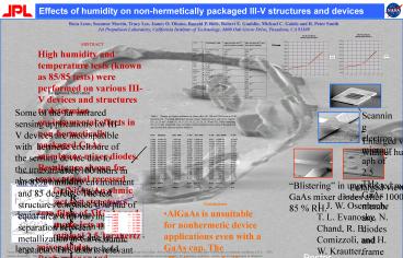
Scanning electron micrograph of 2.5 THz GaAs
membrane diodes and frame prior to humidity
testing. Membranes are 3 microns thick.
Enlarged view of membrane without humidity
testing.
Degradation in contact resistance after 100 hours
in an 85 humidity environment and 85 degrees.
The test structures consisted of a pad of equal
area with varying separation between
metallization in GaAs ohmic contacts. This data
is relevant to both the 640 Ghz and 2.5 Thz mixer
diodes. The contact resistance for these
structures degraded from an average of 5.16 x
10-6 W cm2 to an average of 6.44 x 10⁻⁶ W cm2,
roughly 20. Second set of data shows more
scatter in values but still shows a statistically
significant degradation.
Blistering in unprotected metallization in GaAs
mixer diodes after 1000 hours at 85 C and 85 RH.
Enlarged view of blistered area.
R e s i s t a n c e (W)
References 1. J. W. Osenbach, T. L. Evanosky, N.
Chand, R. B. Comizzoli, and H. W. Krautter,
Temperature-humidity bias behavior and
acceleration factors for nonhermetic uncooled
InP-based lasers Journal of Lightwave
Technology, Vol 15, 861 (1997) 2. Buchhold R,
Nakladal A, Gerlach G, Sahre K, Eichhorn KJ,
Muller M, Reduction of mechanical stress in
micromachined components caused by
humidity-induced volume expansion of polymer
layers, MICROSYSTEM TECHNOLOGIES Vol 5, 3 (
1998 3. R. Manepalli, F. Stepaniak, SA
Bidstrup-Allen, and PA Kohl, Silver
metallization for advanced interconnects, IEEE
Trans. on Adv. Packaging, Vol 22, 4 (1999) 4.
Waters JW et al., The UARS and EOS microwave
limb sounder (MLS) experiments, J. Atm. Sci.,
Vol 56, 194 (1999). 5. Siegel PH, Smith RP,
Gaidis MC, Martin SC, 2.5-THz GaAs monolithic
membrane-diode mixer IEEE Trans. on Microwave
Theory and Techniques, vol 47, 596 (1999). 6. O.
Hallberg and P.S. Peck, Recent humidity
accelerations, a base for testing standards,
Qual. Reliab. Eng. Int. Vol 7, 169 (1991).
Conclusions
- AlGaAs is unsuitable for nonhermetic device
applications even with a GaAs cap. The
effectiveness of other standard passivating films
still remains to be investigated. - 2.5 THz GaAs membrane mixer diodes (with
unpassivated membrane backs) do not show
degradation in their DC I-V characteristics after
500 hours of 85/85 testing. - Process residues can cause morphological changes
(blistering) in exposed areas of GaAs devices
subject to humidity testing. - Unpassivated standard recessed Au/Ge/Ni/Ag/Au
ohmic contacts on GaAs suffer a slight
degradation in contact resitance (Rs). Values
for Rs from different test pads show much greater
variance after the 85/85 tests. Identifying the
cause for this variance will require more
detailed structural characterization like
transmission electron microscopy or scanning
probe microscopy analysis.
Poster background shows crater formed in 1.5
micrometers Al0.98Ga0.02As film capped with a 30
nm GaAs film. Severe film deterioration occurred
after 1000 hours in ambient conditions (25 C,
50 relative humidity). The films that were
subjected to 85/85 testing were totally detached
from the GaAs substrates and consumed by the
resulting oxidation. Crater is 40 micrometers
in diameter.
Poster presented at the 2nd Annual
Microelectronics Reliability and Qualification
Workshop, Oct. 26-27, 1999, Pasadena, CA
Recommended
CrystalGraphics Presentations


