
Status of the SHAFT board design - PowerPoint PPT Presentation
1 / 9
Title:
Status of the SHAFT board design
Description:
It has to be debugged. Next steps: Design the electronic schematic of the board(3 weeks) ... Start the debugging of the prototype ... – PowerPoint PPT presentation
Number of Views:19
Avg rating:3.0/5.0
Title: Status of the SHAFT board design
1
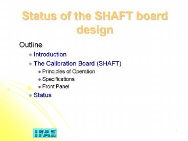
Status of the SHAFT board design
- Outline
- Introduction
- The Calibration Board (SHAFT)
- Principles of Operation
- Specifications
- Front Panel
- Status
2
Introduction
- 3 calibration/monitoring systems to trigger
- CIS (Charge injection system)
- Laser
- MB (Minimum Bias)
- Calibrations can not be done at any moment
- Only during the time that there are no Physical
data acquisition (The LHC machine Gaps) - Design a board to divide the Gaps between the 3
systems (CIS,Laser,MB) and to generate the
calibration triggers for these 3 systems.
3
The LHC Gaps
- LHC Timing pattern
- Orbit time (1 orbit turn) 88.924 us
- The bunches in the LHC are spaced by 25 ns
- But there are missing bunches, so we have empty
bunch crossings (so-called Gaps) - The biggest Gap (3.17 us) is at the cycle end,
and it is made of 127 missing bunches. - Calibration triggers have to be sent during this
Gap.
4
The Calibration Board(SHAFT)
- Triggers will be always sent during the GAP
- Timing between different triggers will be
programmable. - MB trigger needs a dead time of 50 ms just after
a CIS or a Laser trigger to recover the
integrator output and about 50msec before CIS to
recover 3in1 settings.
5
Calibration BoardPrinciples of operation
- Components RAM 4k8bits,12 bits counter,
Shapers(ECL,NIM,LVDS). - Principles of operation
- The pattern RAM is configured from the VME
bus.The value stored at each position of this
memory is used to choose the calibration(MB,Laser,
CIS or none) - The RAM is addressed by the 12 bits counter, and
the counter is increased by the TURN signal.The
TURN signal arrives(from LTP) 1 time each 16
Gaps(orbits) - So at each TURN(1.42mS) one position of memory is
read, and if the corresponding bit is set one of
the triggers(MB,CIS,Laser) will be sent.
6
- The calibration board will be located between the
LTP and the TTCvi - Input Signals BC(clock 40.08MHz),Orbit,Turn,Laser
_Emit,Busy. - Output signals Calibration Request(3 bits),
Laser Trigger, MB Trigger and CIS Trigger. - MB Trigger is sent to one of the BGo inputs of
the TTCvi when TURN signal arrives, and the
corresponding bit of the RAM is set - CIS Trigger is sent to another of the BGo inputs
of the TTCvi when TURN signal arrives, and the
corresponding bit of the RAM is set. 2 pulses are
sent, one to open and the other to close the
charge injection. Cal.Request is also sent to the
LTP. - Laser Trigger is sent to the laser system when
TURN signal arrives, and the corresponding bit of
the RAM is set. The laser system sends back the
Laser emit signal and then the calibration board
sends a Cal.Request to the LTP.
7
Calibration Board Specifications
- The board will be controlled from the VME Bus
- Size 6U VME module
- VME Configuration A24D8D16
- VME Addressing Address Base Offset
- A(23..16)Base address, A(15..0) Offset
- The Trigger pattern is stored in a 4kB RAM
- The RAM is addressed by a 12 bits counter, that
is increased by the TURN signal. - SHAFT I/O Signals
- Input Signals BC(clock 40.08MHz),Orbit,Turn,Laser
Emit, Busy. - Output signals Calibration Request(3 bits),
Laser Trigger, MB Trigger and CIS Trigger.
8
FRONT PANEL
- Total Inputs6 NIM, 1 LVDS, 1 ECL
- Total Outputs9 NIM, 4 LVDS, 2 ECL
9
Status of the Design
- Firmware of the FPGA is almost done
- Little details unknown (polarity of the I/O
pulses, pulse width, etc.) - It has to be debugged
- Next steps
- Design the electronic schematic of the board(3
weeks) - Make the Board layout(3 weeks)
- Manufacture the boards (10 days)
- Solder the boards
- Solder 1 prototype at IFAE (7 days)
- Solder the boards at an external company (3 weeks
or 1 month) - Start the debugging of the prototype
Recommended
CrystalGraphics Presentations


