
Chap. 4: A Systematic Approach to Logic Design - PowerPoint PPT Presentation
1 / 73
Title:
Chap. 4: A Systematic Approach to Logic Design
Description:
Using Digital Circuits to Implement General Algorithms in Hardware ... Introduction to Hardware Design. Classification of Design Methods. Top-down, bottom-up, combined ... – PowerPoint PPT presentation
Number of Views:104
Avg rating:3.0/5.0
Title: Chap. 4: A Systematic Approach to Logic Design
1
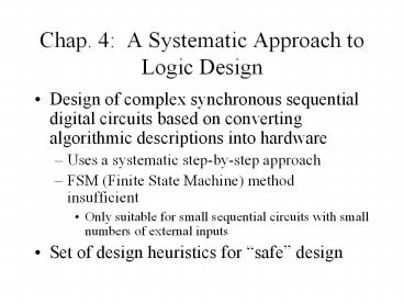
Chap. 4 A Systematic Approach to Logic Design
- Design of complex synchronous sequential digital
circuits based on converting algorithmic
descriptions into hardware - Uses a systematic step-by-step approach
- FSM (Finite State Machine) method insufficient
- Only suitable for small sequential circuits with
small numbers of external inputs - Set of design heuristics for safe design
2
Using Digital Circuits to Implement General
Algorithms in Hardware
- Formal definition of an algorithm
- A general step-by-step procedure for solving a
problem that is CORRECT and TERMINATES. - Informal definition of an algorithm
- A computer-program-like procedure for solving the
problem given. - Algorithm description methods
- Old (outdated) method flowchart
- Pseudocode free-form procedural description
3
ASM (Algorithmic State Machine)
- Originally introduced in 1973 by C. R. Clare
- Example designs
- automatic bank tellers, soccer robot systems,
computers - Advantages
- Uses a systematic S/W-to-H/W conversion method
- Can be used to design large circuits with many
inputs - Disadvantages
- Highly dependent on the use of a graphical
notation called an ASM chart ? cumbersome for
large designs
4
Introduction to Hardware Design
- Classification of Design Methods
- Top-down, bottom-up, combined
- Design Level Hierarchy
- architectural (CPUs, IOPs, memory modules, etc.)
- register-transfer (registers, adders,
counters, etc.) - gate (NAND, NOR, AND, flip-flops, etc.)
- switch (view transistors as voltage-controlled
switches) - transistor (lowest level used in circuit design)
5
VLSI Chip Design versusBoard-Level Design
- VLSI Design (or ASIC Design)
- Full-custom design
- Draw patterns for each individual transistor and
connection - Standard cell based design
- Use a standard cell library (pre-design adder,
counter, etc.) and automatic place-and-route
tools - Board-Level Design
- Produce acceptable design using available parts
(chips) - PCB routing typically done by PCB artwork
experts
6
Design Method Differences
- VLSI Chip Design
- Uses PLAs, transistor-level-designed MSI devices
- Uses latches and multi-phase clocks instead of
FFs - Extremely short signal delays (within the chip)
- Board-Level Design
- Uses mostly standard, off-the-shelf (OTS) chips
- Logic minimization less important than for chip
design - Uses FFs and buffer (transceiver) chips
- Uses PLDs and FPGAs extensively
- Relatively long chip-to-chip signal delays
7
Design Method Similarities
- High-level design is the same
- particularly for synchronous sequential circuits
- ASM-based (modified ASM) high-level design
methodology equally applicable to both - Heuristics for safe design should be followed
for both VLSI chip design and board-level design - use of edge-triggered flip-flops is a possible
exception
8
Partitioning of Digital Circuits
- Control Logic Section
- logic required to generate control signals for
registers, adders, counters, etc. - Datapath Section
- all logic not included in the control logic
section - typically the word-sized data manipulation and
storage components through which the data flows
9
input data
control and status signals
output data
datapath elements
10
Structure of General Digital Circuit
11
Register Transfer Notation (RTN)
- Common notation for describing high-level
behavior of digital systems - Fact All (or almost all) synchronous sequential
digital systems can be viewed as a set of
registers and data transfer operations. - Operations in RTN are always of the form
REGx ? f(REG1, REG2, , REGn)
12
(No Transcript)
13
(Modified) ASM Method
- (1) Pseudocode
- create an algorithm to describe desired circuit
operation - (2) ASM Chart
- convert the pseudocode into an ASM chart
- (3) Datapath
- design the datapath based on the ASM chart
- (4) Detailed ASM Chart
- based on the ASM chart and datapath
- (5) Control Logic Design
14
ASM Chart
- A method for describing the sequential operations
of a digital system - direct conversion from a computer algorithm
- contains all information contained in a state
diagram - Depiction of an ASM chart
- original, graphical notation similar to a
flowchart - tabular notation possible
- text notation possible
15
Original ASM Chart Constructs
dont need
state box
condition box
conditional output
16
ASM Chart Construction Rules
- State boxes should contain only RTN statements
- plus control signals (if necessary)
- All operations within a state box must be
executable in one clock cycle - Combine two state boxes if all operations in both
state boxes can be executed in same clock cycle - Condition boxes should contain only simple
combinational logic queries
17
Example 4.1 ASM Chart
18
Tabular Form of ASM Chart
19
Text Form of ASM Chart
20
Datapath for Example 4.1
21
Detailed ASM Chart
- One-to-one correspondence with ASM chart
- RTN operation ? list of control signals
- unspecified control signals ? default value of
0 - Condition box query ? status signal
- State box contains either
- csig1, csig2, , csigN
- cond(csig1, csig2, , csigN)
22
Detailed ASM Chart for Ex. 4.1
23
Tabular Form of Detailed ASM Chart
24
Text Form of Detailed ASM Chart
25
(Assume C FFH initially)
FFH
(zeroC 1 initially)
26
Control Logic Design Methods
- One-FF-per-state method
- also referred to as one-hot or delay element
method - MUX-based method
- PLD-based method
- results in the most compact implementation
- Sequence-counter method
- for use with cyclical state transition patterns
- outputs of the counter are the control logic
states
27
One-FF-Per-State Method
- Uses one-to-one transformations from detailed ASM
chart constructs to digital logic components - State box transformation
28
- Multiple-path transformation
- Condition box transformation
29
Example of Transformation Process
(D FFs not shown here)
30
(No Transcript)
31
MUX-Based Control Logic Design
32
(No Transcript)
33
PLD-Based Approaches
34
(No Transcript)
35
(No Transcript)
36
Overall (Modified) ASM Process
- Write down a pseudocode solution
- test it out using a short computer program
- Convert the pseudocode to an ASM chart
- try to optimize ASM chart, so it uses few
states - Derive the datapath from the ASM chart
- figure out the datapath components and signals
needed - Form a detailed ASM Chart
- Derive the control logic design
37
ASM Design Example (Drink Machine-Pseudocode)
38
Drink Machine - Detailed ASM Chart
39
Drink Machine - Control Logic
40
ASM Design Example (Light Display-Pseudocode)
41
Light Display ASM Chart
42
Light Display - Datapath
43
Light Display Detailed ASM Chart
44
Light Display Control Logic One FF per State
45
Light Display Control Logic PLD based
46
ASM Design Example (Prob. 4.14)
47
Solution Approach
- Assume input voltage range is 0 , Vmax
- Use a binary approximation algorithm
Actual value
0 Volts
Vmax Volts
Guess 3
Guess 2
Guess 1
48
Step 1 Possible Pseudocode Solution
- While (true) do / all H/W circuits run
infinitely /1. done lt- 02. If (START) then
2.1. done lt- 0 i lt- 7
output lt- 1000 0000 / binary value /
2.2. While (!done) do 2.2.1. If
(greater) then outputltigt lt- 1
else if (less) then outputltigt lt- 0
else / equal /
done lt- 1 2.2.2. If (i gt 0)
then i lt- i - 1 else done
lt- 1 2.2.3. If (!done) then
outputltigt lt- 1
49
(No Transcript)
50
(No Transcript)
51
Step 2 ASM Chart (Text Form)
- s0 done ? 1
- c0 if (START) goto s1 else goto s0
- s1 done ? 0 i ? 7 output ? 80H
- s2
- c1 if (greater) goto s3 else if (less) goto s4
- s3 outputltigt ? 1 if (i gt 0) i lt i 1 else
done ? 1 - if (done) goto s0
- else goto s5
- s4 outputltigt ? 0 if (i gt 0) i lt i 1 else
done ? 1 - if (done) goto s0
- else goto s5
- s5 outputltigt ? 1 goto s2
52
Step 3 Datapath
53
Step 4 Detailed ASM Chart
- s0 setdone
- c0 if (START) goto s1 else goto s0
- s1 cleardone, loadi, initbits
- s2
- c1 if (greater) goto s3 else if (less) goto s4
- s3 setbit, zeroi(countDi), done(goto
s5), done(goto s0) - s4 zeroi(countDi). done(goto
s5), done(goto s0) - s5 setbit, (goto s2)
54
Step 5 Control Logic
55
Overall Design
56
Floating-Point Adder Example
- Dedicated floating-point addition unit for IEEE
standard 32-bit floating-point numbers - Simplify the problem by assuming only positive
floating-point numbers with no special cases - IEEE Standard for floating-point numbers based on
draft proposed by Kahan et. al. in 1979.
57
(No Transcript)
58
Floating-Point Addition Process
59
Step 1 Pseudocode
60
Step 2 ASM Chart
61
Step 3 Datapath
62
Step 3 Datapath, version 2
63
Step 4 Detailed ASM
64
Step 5 Control Logic
65
Derivation of Control Logic Equations
66
Heuristics for Safe Design
- Keep design modular and simple
- Develop good documentation during design
- Use design techniques to avoid clock skew
- Be careful with external asynchronous inputs
- Beware of noise on power and signal lines
- Avoid dependencies on minimum delays
- Initialize all flip-flops to known values
67
Modular Design and Documentation
- Partition complex design into separate modules
- Each module should be separately testable
- Insert test input paths and mechanisms to observe
intermediate signal values - Start with the simplest versions of each module
and follow an iterative design process - Keep good documentation during design process
- net lists, physical placement maps
- HDL (hardware description language) documents
68
Clock Skew
- Clock skews can lead to a violation of the
synchronous circuit assumption and system failure - Example of problem shown in Fig. 4.36 (p. 164)
- Solutions
- Try to equalize wire paths for all flip-flop
clock inputs - Dont use gated clocks
- Use only positive-edge-triggered or
onlynegative-edge-triggered flip-flops
69
(No Transcript)
70
Asynchronous Inputs
- Avoid asynchronous inputs whenever possible
- Buffer remaining asynchronous inputs using FFs
- For critical signals, use debounced switches
- debounced switch circuit shown in Fig. 4.40 (p.
167)
Un-debounced switch circuit
71
Noise and Drive Problems
- Connect all unused inputs to Ground or Vdd
- Use decoupling capacitors between Gnd and Vdd
- about one 0.01-0.1 mF capacitor between all Vdd
and Gnd pins - perhaps one additional large (about 10 mF)
capacitor - Ensure sufficient drive from chip outputs to
inputs - VOHmin gt VIHmin , VOLmax lt VILmax ,
- IOHmax gt S IIHmax at all receivers,
- IOLmax gt S IILmax at all receivers
72
Question How many 74ALS chip inputs can be
driven by one 74AS chip output?
73
- Avoid delay dependencies
- Dont use delay lines (series of inverters used
to create certain minimum desired delays - minimum delays cannot be relied upon
- Delay-insensitive design
- Flip-flop initialization
Recommended
CrystalGraphics Presentations


