
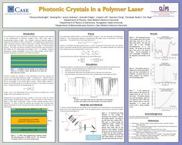
Photonic Crystals in a Polymer Laser - PowerPoint PPT Presentation
1 / 1
Title:
Photonic Crystals in a Polymer Laser
Description:
Another lens collects the sample emission. ... Spectrometer and CCD camera. lenses. sample. half wave plate. on motorized. rotating platform ... – PowerPoint PPT presentation
Number of Views:166
Avg rating:3.0/5.0
Title: Photonic Crystals in a Polymer Laser
1
Photonic Crystals in a Polymer Laser
Thomas Boatwright1, Yeheng Wu1, James Andrews2,
Kenneth Singer1, Joseph Lott3, Hyunmin Song3,
Christoph Weder3, Eric Baer3 1Department of
Physics, Case Western Reserve University 2Departme
nt of Physics Astronomy, Youngstown State
University 3Department of Macromolecular Science,
Case Western Reserve University
Results
Introduction
Theory
- By modeling the electric fields in the device
shown in figure 2, one can calculate its
transmission spectrum. The transmission spectrum
illustrates the band gap, which is important in
the laser application. The electric field in
each layer has a form7 - where xm is the layer boundary position and kmx
is the x component of the wave vector. The
electric field in the slides holding the film is
also accounted similarly. The relation between
the initial and final coefficients can be
represented in matrix form - It can then be shown that the reflectance and
transmittance are
The combination of solid state physics and
Maxwells equations has resulted in the
development of photonic crystals, which offer
novel ways of manipulating a beam of light. The
crystals consist of periodic arrays of
materials with different indices of refraction.
Solving Maxwells equations for these structures
reveals a region where light of certain
frequencies cannot exist, a band gap, similar to
the electronic band gap in semiconductor physics.
This idea of a photonic analog to semiconductors
was pioneered in the 1980s by Eli Yablonovitch
and Sajeev John1,2. In addition, practical
applications being investigated include LEDs,
data storage, optical fibers3, photonic
integrated circuits and nanometer-scale lasers.
a)
b)
3µm defect layer thickness
85µm defect layer thickness
Transmission fraction
b)
Wavelength (nm)
Researchers have applied photonic crystals in
what are known as vertical cavity surface
emitting lasers (VCSELs). Devices similar to
that shown in figure 2 have been constructed,
mostly via spin coating polymers onto a
substrate. In order to lase, the devices are
pumped with a pulsed laser. Lasing thresholds
for such devices have been measured to range from
12-50µJ/pulse.
Materials and Methods
In order to experimentally test the validity of
the simulations, the transmission of the samples
was taken with a Cary Spectrophotometer. From
its measurements, a plot similar to the ones in
figure 3 was produced (see figure 5).
polymethylmethacrylate (PMMA) (n 1.49)
0.255 µm
Figure 4 To determine the lasing threshold of
each sample, an experiment was needed to measure
the emission spectra. The setup on the left
shows how a pulsed YAG OPO laser at 434nm pumps
the multilayered sample. Another lens collects
the sample emission. A detector then sends data
of the spectrum to the computer. A similar setup
was used to find the threshold. To finely tune
the input intensity, a computer controlled
motorized half wave plate between two polarizers
which precisely attenuates the beam.
polymethylmethacrylate (PMMA) doped with C1-RG
fluorescent dye
135 µm
Figure 2 A defect layer sandwiched by 2
photonic crystals with alternating layers of PMMA
and PS. The thicknesses correspond to those in
one of the samples tested.
Recommended
CrystalGraphics Presentations


