
Pcb Layout Design PowerPoint PPT Presentations
All Time
Recommended

An electrical circuitry consisting of embedded metal lines known as traces and bigger metal portions known as planes is located on a solid structure known as a printed circuit board.
| PowerPoint PPT presentation | free to download
ECE-121 TA: Ritu Bajpai Drawing the schematic We have a new version of cadence in the lab now. You will find it listed under ALL PROGRAMS as cadence 16.1 (I am not ...
| PowerPoint PPT presentation | free to download
The designers at PNC have experience with both high power and high frequency RF and microwave PCB layout designs. Because they work closely with the manufacturing team, they know what is possible to achieve with the thick copper layers used in today’s compact LED and motor controllers, and they know what it takes to maintain consistent dielectric properties in the substrates, needed for predictable RF performance. Let them help you with your design.
| PowerPoint PPT presentation | free to download

Synergise PCB Inc, was found in 2002 at USA with a firm commitment to provide best quality PCBs. FPCs & PCBA to match the international standards (IPC Class-II & III) in the designing and manufacturing. Visit: http://synergisepcb.com/
| PowerPoint PPT presentation | free to download

PCB layout performs a primary role in the design for manufacturing of a printed circuit board. The layout procedure produces a visual reflection of the circuits that is essential to manufacture a PCB. Vayo offer design for manufacturing for PCB layout. Contact us today. Vayo Design For Manufacturing: - http://www.vayoinfo.com/
| PowerPoint PPT presentation | free to download

Live project-based PCB & Circuit Design Training in Gurgaon at APTRON is an excellent choice for engineering students and professionals looking to enhance their skills in circuit design and PCB layout. The benefits of this course, such as industry-relevant curriculum, hands-on experience, expert trainers, state-of-the-art infrastructure, and placement assistance, make it a valuable investment in your career.
| PowerPoint PPT presentation | free to download

Altium Designer is considered the epitome of EDA tools for hardware design engineers when it comes to professional schematic and PCB design. It is inclusive and encompassing as far as all the steps in the design and management process are concerned.
| PowerPoint PPT presentation | free to download
PCB is one of the leading PCB suppliers that have provided high quality electronic equipment's for growing industries. We have many years of experience in this field. If you want to take benefit from us then, visit our website.
| PowerPoint PPT presentation | free to download
Microprocessor PCB Design by: Tuan Hung Huynh April 3, 2006 Outline Background Design Process Application Results Purpose Designing computer circuits and software for ...
| PowerPoint PPT presentation | free to download

GREATPCB is a well-known turn-key PCB(1-30 layers) & PCB manufacturing service for low- to mid-volume electronic contract manufacturing, including PCB fabrication, sourcing of components, and complete electronic PCB assembly. With a state-of-the-art facility and modern technology.
| PowerPoint PPT presentation | free to download
PCB Design Services By TronicsZone In Low Cost
| PowerPoint PPT presentation | free to download
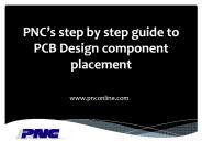
PNC Inc. provides PCB design & layout services from schematics, a sample PC board or films.
| PowerPoint PPT presentation | free to download

If pad is too large may have trouble soldering. Many ECAD systems include solder mask information with the pad files. AED703. 18 ...
| PowerPoint PPT presentation | free to view

VDSM and Full-Custom Layout Design Issues(2)
| PowerPoint PPT presentation | free to view

PCB design & PCB editor courses are conducted by CADD SCHOOL in Chennai. OrCAD software training is provided by CADD SCHOOL in Chennai. CADDSCHOOL is a capture/pspice training institute in Chennai. OrCAD software training is syllabus based and field wise contents are given by CADDSCHOOL in Chennai.
| PowerPoint PPT presentation | free to download

Design for manufacturing, making use of a knowledgeable design staff, improves return on general venture investment by developing efficient, repeatable, trusted items and preventing expensive item problems. Design for manufacturing will improve the high quality of an item from the starting of investment. Vayo provide the best DFM Software, check out design for manufacturing at http://www.vayoinfo.com/
| PowerPoint PPT presentation | free to download

That is our designed purpose of DFT (design for testability). For end customer, the DFT (design for testability) logic present on the device is a repetitive further justify the need of DFT (design for testability) logic, think about an example where an organization needs to offer 1 Million chips to the client. For design for testability contact to vayoinfo @ http://www.vayoinfo.com/design-for-testability/
| PowerPoint PPT presentation | free to download

In easiest form, Design for Testability is a process, which allows a design to turn into testable after production. “Extra” sense which we put combined with the design reasoning during setup process, which helps post-production screening. Post-production testing is required because, the method of developing is not 100% error free. Visit design for testability at http://www.vayoinfo.com/design-for-testability/
| PowerPoint PPT presentation | free to download
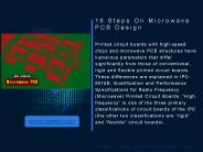
Printed circuit boards with high-speed chips and microwave PCB structures have numerous parameters that differ significantly from those of conventional, rigid and flexible printed circuit boards. These differences are explained in IPC-6018B, Qualification and Performance Specifications for Radio Frequency (Microwave) Printed Circuit Boards. “High frequency” is one of the three primary classifications of circuit boards of the IPC (the other two classifications are “rigid” and “flexible” circuit boards).
| PowerPoint PPT presentation | free to download

Complete report on PCB Design Software market spread across 68 pages providing 4 company profiles and 2 tables and 29 figures is now available at http://www.marketreportsonline.com/contacts/purchase.php?name=567047.
| PowerPoint PPT presentation | free to download

BoardStation / Mentor. Visula / Zuken. STEP-Book AP210. AP214 Interfaces (MCAD) ... pXX / APyyy = ISO 10303 part XX / APyyy (in STEP standard series) ...
| PowerPoint PPT presentation | free to download

From SOLID WORKS cosmos package, 2005, stand alone parts. Analog Board- 195 Hz ... These match very closely to the Solidworks Model as an assembly. ...
| PowerPoint PPT presentation | free to download

... the AP210-based model is much richer than a typical ... Quality Product STEP Data for Exchange Multi-Card Module System Engineering AP 233 AP 210 ...
| PowerPoint PPT presentation | free to download

LQFP quad flat pack (0.8 mm/0.031' pitch) ... SQFP shrink quad flat pack (0.5 mm pitch) TSOP thin small outline packages (0.5 mm pitch) ...
| PowerPoint PPT presentation | free to view

PCB & Circuit Design Training in Delhi at APTRON Delhi is sure to be a game-changer in your journey towards success. So, enroll now and take the first step towards a brighter future in the world of electronics!

PCB Design & Layout Tips Ref: Johnson, H., High-Speed Digital Design. Prentice Hall, 1993 PCB Checklist Do I have header pins for debugging? Do I have convenient VCC ...
| PowerPoint PPT presentation | free to download

GIGABIT ETHERNET DESIGN ... It will be a top concern in the coming week Transmitter Construction & Assembly PCB Design & Layout GIGABIT ETHERNET DESIGN ECE164.02 ...
| PowerPoint PPT presentation | free to download

PCB Manufacture -pcb4u.com. Hardware Design Milestones. Schematic Capture Complete (Feb. 14th) PCB Layout Complete (Feb. 25th) PCB Manufacture (Mar. 6th) ...
| PowerPoint PPT presentation | free to view

Sensor schematics, PCB layouts. Software design documents. Risks involved. Block Diagram ... There are five capacitive circuits on the board. ...
| PowerPoint PPT presentation | free to view

AC PCB Repairing Course aims to bring knowledge of circuit board developing process. The course is specifically designed for one-to-one learners, who want to learn electrical repair and assembly in an easy way. Our AC Repairing course is a comprehensive guide to all aspects of repairing electrical parts. The course teaches the students about different types of board layouts, identification and repair methods.
| PowerPoint PPT presentation | free to download

E906 PAD card PCB layout design, Rev 1.0 Cadence Allegro PCB ESD protection Stage A Stage B Comparator DC/DC converter
| PowerPoint PPT presentation | free to view

High Quality PCB dedicated to excellent services, one stop service ( PCB layout + bare PCB + PCB assembly), prototypes service, mass production service. We solemnly do commitment to you: on time delivery, especially the Quick Turn PCB Prototypes 100% on time delivery.
| PowerPoint PPT presentation | free to download
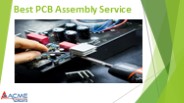
Acme Circuits is known to be amongst the best PCBA manufacturer and exporters in Ahmedabad. Acme Circuits was established in the year 2005 in Ahmedabad, India. Acme Circuits is one of the reputed PCB assembly services providers with complete PCB turnkey solutions. We have been engaged in manufacturing PCB assembly widely used in electronic applications. In Acme Circuits, we acquire international standards to serve the top quality Design as well PCB assembly quality.
| PowerPoint PPT presentation | free to download

Create and run scripts on Expedition PCB layout files ... Verify the Layout with on-line and batch Design Rule Checking. Utilize the Constraint Editor System ...
| PowerPoint PPT presentation | free to view

Title: PowerPoint Presentation Last modified by: xmu Created Date: 1/1/1601 12:00:00 AM Document presentation format: (4:3) Other titles
| PowerPoint PPT presentation | free to download

DL Designs is one of the leading PCB Design companies with clients around the world. Visit our site https://dl-designs.co.uk/
| PowerPoint PPT presentation | free to download

(Monophonic) PCB Design. Improve layout for easier implementation ... Footswitch must be large enough and sturdy enough to be used in a live music situation ...
| PowerPoint PPT presentation | free to download

ATLAS MDT Electronics Status. ASD Chip Design (with ... Mezzanine PCB Design and Production (w/ Harvard) ... Full custom CMOS layout in Agilent (HP) 0.5um ...
| PowerPoint PPT presentation | free to download

Motherboard. FPGA. memory data buffer. memory work space. ethernet ... Status motherboard (in collab. with HD) design and layout done. PCB production in May ...
| PowerPoint PPT presentation | free to view

(Product Design) (Specification Review) (Topology Selection) (Circuitry Design) (Magnetic Devices ...
| PowerPoint PPT presentation | free to download

Based on the industry's market-leading design for manufacturing technological innovation, critical design data is automatically extracted to derive PCB technology classifications for appropriate production process restrictions. Contact for http://www.vayoinfo.com/design-for-manufacturing/
| PowerPoint PPT presentation | free to download

The process of mounting electronic components onto a printed circuit board (PCB). The PCB provides the electrical connections between the components
| PowerPoint PPT presentation | free to download

To find the fuses, switches, and potentiometers, add the discrete library from ... (as recommended by Sara Barnard) Double check 'Gerber Settings' ...
| PowerPoint PPT presentation | free to view

The intersection of mentor Valor DFM and has to spend countless in making procedures, performing DFMs, analyzing feedback optimally, while Layout PCB design, in line with the manufacturer's operational warranty capabilities, has been designed, in phase of process interface model goods, focus on management to make NPI registration process more efficient. Visit NPI software at http://www.vayoinfo.com/ Tag: - NPI software, mentor npi, valor npi, mentor valor dfm
| PowerPoint PPT presentation | free to download

Created webpage. VCSELs. Emcore TO-46, 2.5 Gb/s VCSEL. High performance VCSEL. Costs: Free samples ... initial PCB board layout designs and submit for review by ...
| PowerPoint PPT presentation | free to download

Senior Design Partnership: AmpTraXX2
| PowerPoint PPT presentation | free to download

ITEP Panda PCB for prototype status report by D Malkevich on behalf of the ITEP group ALICE TOF experience - module based on PCB - Module design based on multi layer ...
| PowerPoint PPT presentation | free to download

RayMing is China PCB assembly manufacturer,who offers complete PCB assembly services in Shenzhen, RayPCB’s capable of providing turn-key and partial turn-key printed circuit board assembly services.
| PowerPoint PPT presentation | free to download

Introduction to PCB Design. 2. What is a PCB? Definition: Printed Circuit an electric circuit in which the ... Gull Wing. J-Lead. L-Lead. Flat Lead. Ball ...
| PowerPoint PPT presentation | free to view
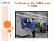
A top-rated company with extensive expertise in assembling PCBs at scale has many attributes. Such a company usually has a good reputation in the competitive global market. The track record is excellent, too. If you are wondering about the benefits of its services, the blog provides a clear overview. Read on! See More: https://fccems.com/product/printed-circuit-board-assembly/
| PowerPoint PPT presentation | free to download
IPC standards are electronic design, manufacturing and inspection standards published by IPC, a global trade and standards setting association focused on the electronics industry. IPC’s standards are used worldwide and have been essential to the globalization of the electronics industry. Anyone who designs or manufactures PCB assemblies needs to be familiar with the standards.
| PowerPoint PPT presentation | free to download

1. DICE board layout (only 2 layers shown) capacitor for instant power temperature sensor resistor ~1cm assumptions for simulations: neglect parasitic capacitance up ...
| PowerPoint PPT presentation | free to download

Background Info. Receiver Soldering and Testing. Optical Link Budget. Vendor Research and Parts. Board Schematic and PCB Layouts. Board Testing. COMING UP NEXT...
| PowerPoint PPT presentation | free to download

(Product Design) (Specification Review) (Topology Selection) (Circuitry Design) (Magnetic Devices ...
| PowerPoint PPT presentation | free to view