
Combinatorial Logic Design Practices PowerPoint PPT Presentation
Title: Combinatorial Logic Design Practices
1
Combinatorial Logic Design Practices
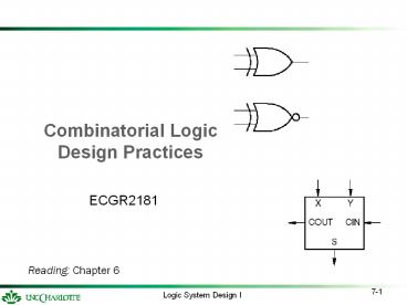
- ECGR2181
Reading Chapter 6
2
Documentation Standards
- Block diagrams
- first step in hierarchical design
- Schematic diagrams
- HDL programs (ABEL, Verilog, VHDL)
- Timing diagrams
- Circuit descriptions
3
Block Diagram
4
Flat schematic structure
5
Hierarchichal schematic structure
6
Other Documentation
- Timing diagrams
- Output from simulator
- Specialized timing-diagram drawing tools
- Circuit descriptions
- Text (word processing)
- Can be as big as a book
- Typically incorporate other elements (block
diagrams, timing diagrams, etc.)
7
Signal names and active levels
- Signal names are chosen to be descriptive.
- Active levels -- HIGH or LOW
- named condition or action occurs in either the
HIGH or the LOW state, according to the
active-level designation in the name.
8
Example
HIGH when error occurs
Logic Circuit
ERROR OK_L
ERROR_L
9
(No Transcript)
10
(No Transcript)
11
(No Transcript)
12
Example Timing Diagram
13
Programmable Logic Arrays (PLAs)
- Any combinational logic function can be realized
as a sum of products. - Idea Build a large AND-OR array with lots of
inputs and product terms, and programmable
connections. - n inputs
- AND gates have 2n inputs -- true and complement
of each variable. - m outputs, driven by large OR gates
- Each AND gate is programmably connected to each
outputs OR gate. - p AND gates (pltlt2n)
14
Example 4x3 PLA, 6 product terms
15
Programmable Array Logic (PALs)
- How beneficial is product sharing?
- Not enough to justify the extra AND array
- PALs gt fixed OR array
- Each AND gate is permanently connected to a
certain OR gate. - Example PAL16L8
16
- 10 primary inputs
- 8 outputs, with 7 ANDs per output
- 1 AND for 3-state enable
- 6 outputs available as inputs
- more inputs, at expense of outputs
- two-pass logic, helper terms
- Note inversion on outputs
- output is complement of sum-of-products
- newer PALs have selectable inversion
17
Designing with PALs
- Compare number of inputs and outputs of the
problem with available resources in the PAL. - Write equations for each output using HDL.
- Compile the HDL program, determine whether
minimized equations fit in the available AND
terms. - If no fit, try modifying equations.
18
Decoders
- General decoder structure
- Typically n inputs, 2n outputs
- 2-to-4, 3-to-8, 4-to-16, etc.
19
Binary 2-to-4 decoder
20
2-to-4-decoder logic diagram
21
Example 2-to-4 decoder
Architecture
22
Decoder Symbol
23
MSI 2-to-4 decoder
- Input buffering (less load)
- NAND gates (faster)
24
Complete 74x139 Decoder
25
3-to-8 decoder
26
74x138 3-to-8-decoder symbol
27
Dataflow-style program for 3-to-8 decoder
28
Dataflow-style program for 3-to-8 decoder
29
(No Transcript)
30
Decoder cascading
4-to-16 decoder
31
More cascading
5-to-32 decoder
32
Decoder applications
- Microprocessor memory systems
- selecting different banks of memory
- Microprocessor input/output systems
- selecting different devices
- Microprocessor instruction decoding
- enabling different functional units
- Memory chips
- enabling different rows of memory depending on
address
33
Example Microprocessor Application
34
Encoders vs. Decoders
35
Binary encoders
36
Need priority in most applications
37
8-input priority encoder
38
Priority-encoder logic equations
39
74x148 8-input priority encoder
- Active-low I/O
- Enable Input
- Got Something
- Enable Output
40
74x148 circuit
41
74x148 Truth Table
42
Cascading priority encoders
- 32-inputpriority encoder
43
Multiplexers
44
Multiplexer - Gate-Level Modeling - Verilog
2-to-1 Multiplexer
// 2-to-1 Multiplexer module module mux_2 (out,
i0, i1, sel) // header input i0, i1, sel //
input output ports output out wire x1, x2,
x3 // internal nets or (out, x2, x3) //
form output and (x2, i0, x1) // i0 ? sel
and (x3, i1, sel) // i1 ? sel not (x1,
sel) // invert sel endmodule
45
Multiplexer - Dataflow Modeling - Verilog
4-bit Multiplexer
// Four-bit 2-to-1 multiplexer module mux_4bit
(Out, A, B, sel) input 30 A, B input
sel output 30 Out assign Out sel ? B,
A endmodule
46
Multiplexer - Behavioral Modeling - Verilog
Conditional Statements
module mux4_to_1 (A, B, C, D, OUT, select) input
70 A, B, C, D input 10 select output
70 OUT reg 70 OUT always _at_ (A or B or C
or D or select) case (select) 2d0 OUT A
2d1 OUT B 2d2 OUT C 2d3 OUT
D endcase end
47
74x1518-input multiplexer
48
74x151 truth table
49
CMOS transmission gates
- 2-input multiplexer
50
Other multiplexer varieties
- 2-input, 4-bit-wide
- 74x157
- 4-input, 2-bit-wide
- 74x153
51
Barrel shifter design example
- n data inputs, n data outputs
- Control inputs specify number of positions to
rotate or shift data inputs - Example n 16
- DIN150, DOUT150, S30 (shift amount)
- Many possible solutions, all based on multiplexers
52
16 16-to-1 muxes
16-to-1 mux 2 x 74x151 8-to-1 mux NAND gate
53
4 16-bit 2-to-1 muxes
16-bit 2-to-1 mux 4 x 74x157 4-bit 2-to-1 mux
54
Properties of different approaches
55
2-input XOR gates
- Like an OR gate, but excludes the case where both
inputs are 1. - XNOR complement of XOR
56
XOR and XNOR symbols
57
Gate-level XOR circuits
- No direct realization with just a few transistors.
58
Equality Comparators
- 1-bit comparator
59
8-bit Magnitude Comparator
60
Other conditions
61
Adders
- Basic building block is full adder
- 1-bit-wide adder, produces sum and carry outputs
- Truth table
62
Full-adder circuit
63
Ripple adder
- Speed limited by carry chain
- Faster adders eliminate or limit carry chain
- 2-level AND-OR logic gt 2n product terms
- 3 or 4 levels of logic, carry lookahead
64
74x2834-bit adder
- Uses carry lookahead internally
65
(No Transcript)
66
Ripple carry between groups
67
Lookahead carry between groups
68
Subtraction
- Subtraction is the same as addition of the twos
complement. - The twos complement is the bit-by-bit complement
plus 1. - Therefore, X Y X Y 1 .
- Complement Y inputs to adder, set Cin to 1.
- For a borrow, set Cin to 0.
69
Full subtractor full adder, almost
70
Multipliers
- 8x8 multiplier
71
Full-adder array
72
Faster carry chain
Recommended
