
JEOL JBX5000LS PowerPoint PPT Presentation
1 / 90
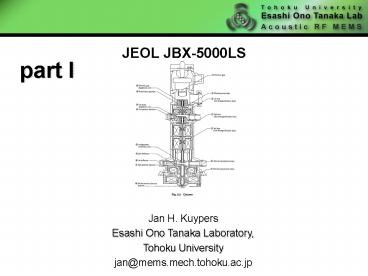
Title: JEOL JBX5000LS
1
JEOL JBX-5000LS
part I
Jan H. Kuypers Esashi Ono Tanaka
Laboratory, Tohoku University jan_at_mems.mech.tohoku
.ac.jp
2
contents part I
- motivation
- electron sources
- electron optics
- electron-solid interactions
- realistic resolutions
- EB resist
- exposure scheme
- exposure dose calculation
- JEOL stage layout
- handling proximity effects
3
motivation of EB
- reason to use electron beam lithography ?
- want to make small patterns
- Why do we use electrons ?
- quantum mechanics
- de-Broglie wavelengths every particle can be
described by its de-Broglie wavelenghts
4
motivation of EB
- de-Broglie wavelenghts of an electron
- for an electron being accelerated by a voltage
Vacc V we find - example
- Vacc 50 kV ? le,50kV 5.49 pm
- resolution limit in optical lithography (OL)
limited by diffraction - electron beam lithography not limited by
diffration!!! (or we could write pm-order!!)
5
EBL
6
EBL why we use it
- of course we could use
- DUV state of the art semiconductor lithography
systems - price
- personnel
- (the NIKON stepper (VBL) can maybe achieve 400
nm) - SPM technology (surface probe technology)
- very slow
- very high defect rate
- reproducibility bad
- ? EBL is the most available technology we have
7
- EBL basics and theory
8
typical EBL system
- general simplified layout
9
detailed layout
- we will try tounderstand this
10
- electron sources
11
electron emission
- emission methods
- thermionic
- heating of filament? electron energy exceeds
work function? electron emission
12
electron emission
- field emission
- sharp tip Rlt1µm (tungsten needle)
- very high electrical field at tip extracts
electrons - cold emission
- drift
- short term noise
- cause atoms adsorbing on the tip ? affects work
function and thus emission? flashing (short
heating can clean it), but atoms re-adsorb - atoms also ionized and sputter the tip
- ? requires vacuum of lt10-10 Torr!!!!!
- CFE has not found application in EBL
13
electron emission
- thermal field emission ( Schottky Emitter)
- mixture of thermionic and FE
- heating of tungsten needle 1800K (not 2700K)
- less sensitive to gases
- stable for several months
- tip coating with ZrO to reduce work function
- vacuum required 10-9 Torr (readily achievable)
14
the JEOL JBX-5000 LS
- thermionic (traditional/oldest)
- our JEOL JBX-5000LS is also thermionic
- principle
- current heats emitting material to emit electrons
- common materials
- tungsten (W)
- most common/first material
- not very bright
- requires large temperature (2700K)? large energy
spread - Lanthanum Hexaboride (LaB6) ? our system
- low working function
- high brightness (at 1800K)
- higher beam current achieved by higher filament
heating current - larger energy spread
- reduces lifetime of filament (evaporation of
material)
15
JEOL EB LaB6
- by DENKA
- orientation lt100gt
- tip angle 90
- tip radius 15 µm
- price 900.000 Yen (8000 US)
- should be exchanged 4x/year
16
properties of electron sources
17
filament setup
our system
18
JBX 5000 filament setup
19
electron optics
until here should be clear
20
electron optics
- electron lenses
- magnetic
- electrostatic
- properties
- not as good as optical lenses
- poor quality of these lenses leads to
- restricts field size (how large a range can be
exposed without moving the stage by deflecting
the electron beam our system 80x80 µm) - convergence angle (numerical aperture)
- critical deviations
- spherical aberration
- outer zones of the lense focus more strongly
- chromatic aberrations
- (optics wavelength, recall de-Borglie ?
electron energy/spread) - electrosn with different energies focused at
different image planes - solution
- reduce convergence angle ? electrons confined to
centre (by small apertures) - disadvantage reduces the beam current drastically
21
magnetic lens
- copper windings surrounded by circularly
symmetric iron (or other high permeability
material) - electrons experience Lorentz-force
- focusing sequence
- electrons start to rotate (cork screw)
- rotation component and B-field force electrons to
the centre - this rotation of the electron beam is later
corrected during beam conditioning
22
electrostatic lens
1.
2.
- inner potential controls lens strength
- electrons travelling away from the optical axis
- 1. attracted and pulled inwards
- 2. repelled by second electrical field from
bottom ground electrode - electrostatic abberations worse than magnetic
- often used in a condenser lense
- abberations dominated by last lens
23
electron optics
5 magneticlenses principle as explained
24
apertures
- small holes through which the electrons pass
- used in
- beam limiting aperture
- to limit the beam convergence angle a
- to limit beam aberrations
- to set the beam current
- beam blankers (blanking aperture)
- used to turn the beam on and off
25
JEOL apertures
- restriction aperture
- as close to e-gun as possible
- prevents space charge effects? electron
repulsion(electrons charge up non grounded parts
in the column ) - position can not be changed
electron beampasses throughthese holes
26
JEOL apertures
- 1st aperture selector
- intended for
- aligning the electron beam to the optical axis of
the system - (stopping the beam mechanically)
see beam blanking(later)
electron beam passes through these holes
27
JEOL apertures
- 2nd aperture selector
- intended for
- adjustment of objective aperture position
- aligning the electron beam to the optical axis of
the system
electron beam passes through these holes
28
electron optics
fixed, can not be changed
can be adjusted
29
JEOL apertures final
- problem of contaminated apertures? degrade
resolution - are changed every time the system is mainatained
by JEOL engineers (few month)
30
beam defelectors
- for scanning of electron beam across our sample
- causes additional aberrations
- outer area most affected
- magnetic better than electrostatic
- often 2 coil pairs used? featuring less
aberrations - electrostatic deflection faster (coil inductance
limits frequency responseeddy currents)
scaned EB
31
beam blanker
- beam blanking (switching beam on or off)
- pair of plates working as electrostatic deflector
- to turn beam off voltage applied between plates?
beam pulled away from optical axis - must operate at very high speed
- would leave streaks in our resist pattern, so
- often built around crossover point or
intermediate focal point (conjugate blanking)?
spot does not move on wafer plane
V
-V
beam leavesstreak to the left
32
beam blanker
- conjugate blanking
- blanking plates built around crossover point or
intermediate focal point - 1. beam pulled outwards
- 2. beam focused more strongly
- 3. focus plane does not change
- possibly
- due to aberrations slight increase of beam size
33
electron optics
- beam blanker
34
JEOL blanking unit
- blanker operation frequency 6 MHz
- minimum exposure time 167 ns
- consequences later
35
stigmator
- corrects imperfections of
- construction of EB column
- alignment of EB column
- resulting in astigmatism
- result
- round beam becomes ellipse
- images is blurred
- stigmator forces beam back to optimum round shape
36
stigmator
- layout
- usually electrostatic or magnetic
- 4 or usually 8 poles around optical axis
37
electron optics
- stigmator
38
operation of JEOL EB
- you only have to set
- gun alignment (G-Al)
- only X,Y shift (HORIZ)
- 1st alignment (1-Al)
- only X, Y TILT
- set
- tilt
- shift
Tilt
Shift
39
G-Al and 1-Al
- JEOL operation
40
EB column review
41
EB column review
42
EB column review
43
EB column review
44
lithography operation
- JBX-5000LS
- two projection lenses (4th and 5th)
- uses either lens depending on
- resolution
- writing time (larger beam ? faster, using larger
beam current)
45
discussion
- learnt so far
- what parts are in the EB column
- what they do
- their principles
- ? we are getting closer to practice
- what is the resolution ?
46
- beam sizes and pattern sizes
- the whole story
47
resolution
- for perfect e-opticsdivide virtual source size
by demagnification - however
- far from perfect lens aberrations (spherical,
chromatic)
example not related to our JEOL
lens aberrations improve forsmaller convergence
angle
theoretical limitsource size/magnification
48
resolution JEOL
- beam sizes for our JEOL JBX-5000 LS
- larger current ? more filament heating? larger
energy spread - larger current leads to larger Coulomb repulsion
? beam widening
5th lens largest demagnification
1040 nm
49
resolution JEOL
- beam sizes for our JEOL JBX-5000 LS
- using the 4th lens
40250 nm
50
resolution JEOL
- beam sizes for our JEOL JBX-5000 LS
- beam current vs beam size
- 30 pA 13 nm beam size
- 100 pA 20 nm beam size
- BUT
- machine specs for perfect alignment
- perfect temperature control
- perfect maintainance
- depends very much on filament condition
- JEOL recommendation change 4x/year
- we only change 1x/year (1000.000 Yen, 8000 US)
- the other bad news
- beam size ? pattern size
51
- electron physics(or what happens after the
eltrons leave the column)
52
electron-solid interactions
- electron scattering
- slight scattering in resist? forward scattering
- large angle scattering events in substrate?
backscatteringleads to dose from near by
structure? proximity effect - electrons slow down producing cascade of low
energy electrons (secondary electrons)
53
electron scattering
- larger acceleration voltage
- reduces forward scattering
- reduces backscattered dose at substrate surface
54
forward scattering
- forward scattering formula (honto ??!)
- increase in beam size (Dx) due to forward
scattering in nm - where
- tr resist thickness in nmVacc accleration
voltage - example
- resist thicknes ZEP520A 400 nm, Vacc 50 kVDx
20 nm beam broadening from top of resist to
bottom
55
forward scattering
- forward scattering and resist profile
- depending on development time and forward
scattering - resist profile can be controlled
- changes from positive to negative slope
- e.g. negative slope ideal for lift-off
increasing development time
posite typeEB resist
substrate
56
backscattering
- higher atomic materials lead to larger scattering
- often substrate determined by process (Si)
- ratio of backscattered electrons as h
- typical values
- 0.17 for silicon
- 0.50 for tungsten or gold
- scattering range large 520 µm
57
proximiy effect example
58
secondary electrons
- during primary electrons slowing down energy
dissipated in form of secondary electrons (2-50
eV) - these secondary electrons are responsible for the
actual resist exposure - their range in the EB resist is 10 nm
- this limits practical minimum resolution of even
the best systems to 20 nm!!!(not including
forward scattering!)
59
final discussion
- what is the best we could get ?
- beam size (50 kV, 30 pA) 13 nm
- forward scattering (100 nm resist) 2.6 nm
- SE range (10 nm) 20 nm
- the theoretical size with a new filament and best
conditions could be 35.6 nm - If you can write under 50 nm (repeatedly) with
our JEOL system I will by you a crate of beer!
60
- EB resist
61
typical resist
62
generally
- positive type resist
- polymer back bone broken by electron irradiation
- most posi resist have bias of 20150 nm(i.e.
hole in resist larger than electron beam size) - negative resists
- cross-linking of polymer chains
- smaller bias (often zero)
- problems with
- scum (insoluble residue in exposed areas)
- swelling during development
- brdiging between features
63
discussion
- experience with
- ZEP520A (posi)
- SAL-601 (nega)
- higher resolution with positive type ZEP520A
- please read datasheets for more information
- resist thickness
- spin curves
- thinner
- safty etc
- EB resist contain a lot of solvent(thats why
they turn out so thin) - please always ware a gas-mask for your own
health when spin-coating
64
how to check your results ?
- I have written an EB pattern, how do I check it ?
- SEM
- be careful EB resist is sensitive to eletrons -
) - ZEP520 and PMMA will swell and lines will shift
under high magnification SEM viewing!!! - ? solution
- either etch into the substrate
- lift-off metal pattern
- ZEP will swell under high
- AFM
- user dicer marks on backside of sample to cleave
samples to small size required for AFM - make macroscale marks indicating the position of
your nanoscale pattern - again step heights of gt50 nm are hugh for an
AFM!!! - shallow etch probably best
- your way ? write on WIKI
65
dielectric samples
- charge up of
- dielectric wafers
- top layer is dielectric
- ? use e-spacer
- conductive layer 10 nm
- spin on after EB resist coating
- remove with DI water rinse
66
spin coating
- EB sample sizes must be(we only have those
holders) - 20 x 20 mm
- 20 x Y mm (where 17 ltY lt 20 mm)
- 2 wafer
- 3 wafer
- use primer
- HMDS (OAP)
- resist stored in fridge
- takes 10 min to warm to room temperature(do
Never open faster than that? condensation in
bottle will occur, reduces shelf-life) - very expensive (100cc 500.000 Yen, 450 US)
- dehydration bake (180C)
67
- JEOLs exposure strategy
- (how your pattern is written and how it affects
your pattern)
68
EB dose
- electron beam dose Q µC/cm2
- exposure time given as
- where
- Q the exposure dose
- I beam current
- A the area exposed
- example
- Q 80 µC/cm2
- I 30 pA
- A 10 x 10 mm
- ? t 2667 s 45 min (without stage movent etc.)
69
JEOL EB writing
- JEOL EB
- rasterizes your data
- raster size x (usually 1.25 nm)
- exposure of single dots
- exposure dose for the JEOL is set by determining
the dwell time of each dot - this dwell time must be larger than 167
ns(minimum beam blanking time) - if the dwell time is smaller than 167 ns,
skip-steps k have to be inserted
70
JEOL EB writing
- dwell time is calculated with
- where
- Q the exposure dose µC/cm2
- I beam current nA
- k skip steps necessary
- n beam address grid in steps per micron
(usually 800, because x 1.25 nm) - example
- Q 80 µC/cm2
- I 100 pA
- result due to minimum dwell time of 167 ns, k
4 - ? td 200 ns
71
dwell time calculation
- dwell time calculator program
- freely distributed to all JEOL EB users
72
- JEOLs EOS
- Electron Optics System
73
EOS table
- we usually use EOS mode 8 and the 5th lens for
exposure - grid is 1.25 nm (800 steps per micron)
- EB can expose a field size of 80 x 80 µm without
moving the stage
74
EOS 8-x
- settings of the electron optics are saved in an
EOS database - coding X, Y or X-Y
- where X stands for the EOS mode
- mostly X 8, (5th lens highest resolution)
- Y stands for the user or laboratory ID
- e.g. 8-5 is for Esashi lab
- 8-6 is for Hane lab etc.
- your settings will overwrite the settings of all
user in your lab!!! - this includes
- beam current (Esashi lab standard 100 pA)
- the wafer centre position
- alignment marks settings
- ? please be careful
75
- JEOL stage layout
76
JEOL stage
X
Y
wafer holder loaded for every exposure
does not leavemain chamber attached to stage
77
stage inside machine
78
JEOL stage
- controlled by laser interferometer
- stage position units 0.62 nm
- resolution of interferometer l/1024
X-axis
Y-axis
79
sample holder
1. set wafer/samples on holder
2. load holder into cassete
3. set in load lock chamber
80
- handling electron scattering(additional slides)
- method proposed by
- J. H. Kuypers,
- Esashi Ono Tanaka Laboratory,
- Tohoku University
81
scattering function
- electron scattering
- forward scattering
- backscattering
- dependence
- materials thickness
- beam current
- acceleration voltage
- development/process
- ? proximity function
82
scattering function
- double Gaussian function
- forward scattering
- backscattering
- can include developing time and subsequent
process (etching or lift-off) - requires
- a forward scattering coefficient
- b backscattering coefficient
- h ratio of backscattered electrons exposung
resist - Qc critical dose
83
scattering solution
- how to improve these effects ?
- do not put large structures beside small
structures - evaluate scattering parameters
- simulate your CAD and addapt it
84
my method
- this is my genuine method
- feel free to use it (and thanks for the credits)
- EB dose distribution calculated mathematically
by - convolution of CAD pattern and beam dose
distribution
85
line eval method
- design array of lines
- dimensions as close to your desired size
- length longer than 2x 3b ( 3s of backscatter
Gaussian), usually b 3-10 µm - measure width of lines with SEM (takes a long
time - (because lines longer than 2x 3b, lines
are infinetly long!
86
my test pattern
- evaluate
- different doses
- different development times
- ? these conditions must be fixed!
- my recommendation
- do not use agitation during development, it will
not be repeatable
87
my test pattern
- design different line and space ratios
- measure with SEM
- to compensate for scale effects in SEM measure
pitch of lines (not affected by scattering!) - use this as weigting factor to get true size
88
evaluation
- measured line width for different line/space
ratios - to remove noise for fitting, use 12th order
polynom best fit (as shown)
89
fitting the parameters
- as lines are infinetly long problem reduced to 1D
- use linearity of convolution
90
EB dose adaption
- compute best fit
- simulate pseudo 2D dose simulation of your CAD
- addapt your CAD
- you will like the result - )
direct CAD
compensated CAD
Recommended
