
Large-Area%20Micro-pore%20Photo-sensors - PowerPoint PPT Presentation
Title:
Large-Area%20Micro-pore%20Photo-sensors
Description:
LargeArea Micropore Photosensors – PowerPoint PPT presentation
Number of Views:111
Avg rating:3.0/5.0
Title: Large-Area%20Micro-pore%20Photo-sensors
1
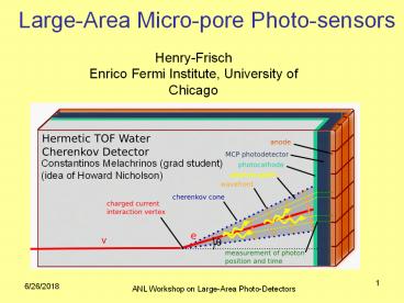
Large-Area Micro-pore Photo-sensors
Henry-Frisch Enrico Fermi Institute, University
of Chicago
Constantinos Melachrinos (grad student) (idea of
Howard Nicholson)
2
Large-Area Micro-pore Photo-sensors OUTLINE
- Basic ideas- small characteristic size,
homogeneity, scalability, integrated low-power
cheap electronics. - Parameters tuneable to application- space/time
resolution, occupancy, readout deadtime, cost. - Status and proposed time-line for development?
- Typical expected performance
- Application to a water Cherenkov counter (also to
Liquid Argon?) - Possible Opportunities
- Hermetic- close to 100 coverage?
- Reduced cost of PMs for same volume
- More opportunities for cavern aspect ratio/
fiducial volume - Robustness against pressure, magnetic field?
- Tracking detector- possible track/vertex
reconstruction? - Sign determination (weak field)??
3
Large-Area Micro-pore Photo-sensors WHAT THIS
IS NOT
- A proposal for an alternative to the baseline
detector - A mature collection of thoughts
- A description of a well-understood technology
- A plan with a schedule and resource requirements
- Any attempt to get in the way of making DUSEL
real.
WHAT THIS IS
- A response to new RD on large-area psec
photo-detectors started for collider applications
and PET, and enabled by new developments in
front-end electronics. - An investigation into a possible application of
large-area fast photo-detectors to a
high-priority US project. - An exploration of the parameter space for water
Cherenkov neutrino detectors- coverage,
resolution,.. - An effort that would have a lot of spin-offs for
society.
4
Why has 100 psec been the for 60 yrs?
Typical path lengths for light and electrons are
set by physical dimensions of the light
collection and amplifying device.
These are now on the order of an inch. One inch
is 100 psec. Thats what we measure- no surprise!
(pictures from T. Credo)
Typical Light Source (With Bounces)
Typical Detection Device (With Long Path Lengths)
5
Solving the Small/large Problem
- RF Transmission Lines as anodes
- Small features for amplification- Homogeneous
- Large transverse size for readout is pulse
shape-preserving - Readout both ends of transmission lines
- Work on leading edge- ringing not a problem for
this fine segmentation
6
Characteristics we need
- Feature size lt 300 microns ( 1 psec at c)
- Homogeneity (ability to make uniform large-area-
think amorphous semicndtr solar-panel) - Fast rise-time and/or constant signal shape
- Lifetime/robustness/simplicity
- Cost/unit-area ltlt that for photo-multipliers
7
An Explanation of what follows
- Ive been driven by wanting to follow flavor-flow
in colliders- most of our work has been focused
on that geometry- light made in window by a
relativistic particle, 30 photo-electrons, goal
of lt 1 psec timing. Youll see most results for
this regime- have to scale back to single photons - Havent thought much at all about applying this
to neutrino detectors- Howard Nicholson suggested
it while listening to a talk. Hence this
workshop. - Note- good time and space resolution come
naturally in this design- get 3D (tomographic)
info by design.
8
Detector Development- 3 Prongs
- 1. Electronics- have settled on wave-form
sampling - Already demonstrated by Breton, Delanges,Ritt,
and Varner- many pieces exist, main change is
going to faster process and pooling expertise. - Reasonable precision (see talk at Lyon by Genat)-
few psec with present rise times, 1 with faster
MCP design. - Gives much more than time- space, pileup, etc.
(Tang Lyon talk) - 2. MCP development- techniques and facilities
(probably) exist- ALD, anodic alumina--will
require industry, natl labs, - 3. Simulation
- Electronics simulation in good shape
- Rudimentary end-to-end MCP device simulation
exists- starting up with commercial packages
(SimIon, CPO, ) - Validation with laser teststand and beam line
started
9
GOAL to Develop Large-Area Photo-detectors with
Psec Time and mm SpaceResolution
Too small- can go larger- (But how does
multiplication work- field lines?)
From Argonne MSD ALD web page- can we make cheap
(relatively) ultra-fast planar photo-detector
modules?
10
Generating the signal for relativistic particles
(HEP, nuclear, astro, accelerator- but different
for neutrinos)
Incoming rel. particle
- Use Cherenkov light - fast
Custom Anode
Present work is with commercial MCPs e.g.
Burle/Photonis Planicons. Expensive (!), hard to
get, little flexibility. BUT- it works. And well.
11
Design Goals
- Colliders 1 psec resolution, lt 100K/m2
- Neutrino H2O 100 psec resolution, lt 1K/m2
- PET 30 psec resolution, lt 20 of crystal cost
Micro-photograph of Burle 25 micron tube- Greg
Sellberg (Fermilab)- 2M/m2- not including
readout
12
Proof of Principle
- Camden Ertley results using ANL laser-test stand
and commercial Burle 25-micron tube- lots of
photons - (note- pore size may matter less than current
path!- we can do better with ALD custom designs
(transmission lines))
13
Understanding the contributing factors to 6 psec
resolutions with present Burle/Photonis/Ortec
setups- Jerry Vavras Numbers
- TTS 3.8 psec (from a TTS of 27 psec)
- Cos(theta)_cherenk 3.3 psec
- Pad size 0.75 psec
- Electronics 3.4 psec
14
Photo-multiplier in a Pore
- Idea is to build a PMT structure inside each
pore- have a defined dynode chain of rings of
material with high secondary emissivity so that
the start of the shower has a controlled geometry
(and hence small TTS) - One problem is readout- how do you cover a large
area and preserve the good timing? - Proposed solution- build anode into pores,
capacitively couple into transmission lines to
preserve pulse shape.
15
Psec Large-area Micro-Channel Plate Panel (MCPP)-
LDRD proposal to ANL (with Mike Pellin/MSD)
N.B.- this is a cartoon- working on workable
designs-join us
Front Window and Radiator
Photocathode
Pump Gap
Low Emissivity Material
High Emissivity Material
Normal MCP pore material
Gold Anode
50 Ohm Transmission Line
Rogers PC Card
Capacitive Pickup to Sampling Readout
16
Get position AND timeAnode Design and
Simulation(Fukun Tang)
- Transmission Line- readout both endsgt pos and
time - Cover large areas with much reduced channel
account.
17
Photonis Planicon on Transmission Line Board
- Couple 1024 pads to strip-lines with
silver-loaded epoxy (Greg Sellberg, Fermilab).
18
Photonis Planicon on Transmission Line Board
Ed May, Jean-Francois Genat- a week ago
- Left laser on one spot Right laser then moved
over 10 mm and plots superposed. (3.1 psec/count-
last week)
19
Comparison of measurements (Ed May and
Jean-Francois Genat and simulation (Fukun Tang)
- Transmission Line- simulation shows 3.5GHz
bandwidth- 100 psec rise (well-matched to MCP) - The time difference yields a velocity of 64ps/cm
against 68ps predicted
20
Scaling Performance to Large AreaAnode
Simulation(Fukun Tang)
- 48-inch Transmission Line- simulation shows 1.1
GHz bandwidth- still better than present
electronics.
21
Front-end Electronics
Critical path item- probably the reason psec
detectors havent been developed
- We had started with very fast BiCMOS designs- IBM
8HP-Tang designed two (really pretty) chips - Realized that they are too power-hungry and too
boutique for large-scale applications - Have been taught by Gary Varner, Stefan Ritt,
Eric DeLanges, and Dominique Breton that theres
a more clever and elegant way- straight CMOS
sampling onto an array of capacitors - Have formed a collaboration to do this- have all
the expert groups involved (formal with Hawaii
and France)- see talks by Tang and Jean-Francois
at Lyon
22
FY-08 Funds ChicagoAnode Design and
Simulation(Fukun Tang)
23
Front-end Electronics
- Wave-form sampling does well- CMOS (!)
24
Front-end Electronics- Schedule
- Collaboration with ANL, UC,Hawaii, Orsay, Saclay,
and advise and wisdom and parts from PSI gt have
all 4 sampling groups. J-F in France now with
them. - Have proposed 3 ½ year schedule for completion of
0.13 micron 40-GS/sec ASIC for collider and other
relativistic particle applications. - Present chips probably adequate for neutrino
application- dont need few psec resolution- have
new PSI DRS4 on its way to UC now chips from all
gps in use in running experiments - Needs a needs assessment- but no show stoppers...
25
Modus Operandi so far
- In Nov. 2005, we had our 1st workshop- idea was
to invite folks working or interested in related
subjects- didnt know many (most) of them - Have developed tools and knowledge- also contact
with pioneers and practictioners (Ohshima,
Howorth, Vavra, Breton, Delanges, Ritt,
Varner) - Development clearly too big for one group-
devices, electronics, applications- have worked
collaboratively with each other, national labs
(see talks by Karen, Andrew,Jerry,), and
industry (Burle/Photonis, Photek, IBM,)
26
Development of the Device
- Started effort with ANL HEP, Materials Science,
and Energy Systems Divisions - Have started investigating AAO using facilities
of Center for Nano-scale Materials
Hau Wang (ANL/MSD) First try- not final pores or
final process but shows what they can do quick..
27
Development of the Device
- Schedule- working on making a resource-loaded
schedule - Workshop at end of February dedicated to device
development - Idea is to have a preliminary plan by end of
workshop real plan by early summer - Do relativistic particle, single-photon, and PET
in parallel until paths diverge. - My hope is that its 3-4 years.
28
Application to a water Cherenkov Counter- effect
on the physics
29
Application to a water Cherenkov Counter- effect
on the physics
- What does coverage buy ?
- What does spatial resolution in x-y buy?
- Can x-y-z resolution allow track reconstruction?
- Can x-y-z resolution allow pizero-electron sep?
- Can one get momentum from multiple scattering?
- What are the trade-offs in geometry if you have
robust (pressure-resistant) detectors? (Mayly) - What havent we thought of? (e.g. magnetic field
for sign determination).
30
Schedule and Milestones (?)
- Small (1) AAO with pores- started (Hau)
- Same with ALD- tests of gain
- Same with photo-cathode and anode- laser tests
- 2 x 6 AAO with pores
- Same with ALD- tests of gain
- Same with photo-cathode and anode
- Same with sampling chip readout (chip started)
- 8 x 8 (or so- a floor-tile)- same steps
- In parallel of latter, commercialization (NDA
signed). - 4 years??? Depends on talent, resources,
investment- many details- but many indications
its possible.
31
Thank you
32
My Questions This Time-INote- many questions
from previous workshops have been answered!
- What is the electric field geometry in the MCP
pore? (what are bulk and surface resistivities?
). - What is the response of a nano-carbon film to 200
eV electrons? (photons?) - After the first strike, can the pore be straight?
- If one uses diamond (e.g.), do you really need
fewer strikes?
33
My Questions This Time-IINote- many questions
from previous workshops have been answered!
- Other ways to make pores- e.g. Pierre Jarrons
developments? - Who makes big photocathodes? (Pioneer?)
- Who is interested in learning how to make big
photocathodes for fast timing? - Is there a simulation of the internal workings of
photo-cathodes out there somewhere?
34
My Questions This Time-III
- Can we get a serious simulation effort of the MCP
functions started (collab with Lyon?)? - Funding from NSF Computing, SBIR, a a a a a
European agency? - Are there MCP simulations already out there?
- Can we find a Materials Science group with
students, postdocs, etc. to work with us?
35
Simulation and Measurement
- Have started a serious effort on simulation to
optimize detectors and integrated electronics - Use laser test-stands and MTEST beam to develop
and validate understanding of individual
contributions- e.g. Npe, S/N, spectral response,
anode to input characteristics, - Parallel efforts in simulating sampling
electronics (UC, Hawaii) and detectors
(UC,Saclay, Tom Roberts/Muons.inc).
36
Argonne Laser Lab
- Measure Dt between 2 MCPs (i.e root2 times s)
no corr for elect. - Results 408nm
- 7.5ps at 50 photoelectrons
- Results 635nm
- 18.3ps at 50 photoelectrons
37
Work in Progress
- Our way of proceding- use laser test-stand for
development, validation of simulation- then move
to testbeam for comparison with simulation with
beam. - Changes to electronics readout
- Add Ritt and/or Varner sampling readouts
(interleave 10 GS) in works - First test via SMA then integrate chips onto
boards? - Development of 40 GS CMOS sampling in IBM 8RF
(0.13micron)- proposal in draft (ANL, Chicago,
Hawaii, Orsay, Saclay) - Changes to the MCPs
- 10um pore MCPs (two in hand)
- Transmission-line anodes (low inductance-
matched)- in hand - Reduced cathode-MCP_IN MCP_OUT-anode gaps-
ordered - ALD module with integrated anode and capacitive
readout- proposed (ANL-LDRD)
38
Psec Large-area Micro-Channel Plate Panel (MCPP)-
LDRD proposal to ANL (with Mike Pellin/MSD)
Front Window and Radiator
Photocathode
Pump Gap
Low Emissivity Material
High Emissivity Material
Normal MCP pore material
Gold Anode
50 Ohm Transmission Line
Rogers PC Card
Capacitive Pickup to Sampling Readout
39
FY-08 Funds ChicagoAnode Design and
Simulation(Fukun Tang)
40
Jerrys s re-visited Solutions to get to
ltseveral psec resolution.
- TTS 3.8 psec (from a TTS of 27 psec)
- MCP development- reduce TTS- smaller
pores, smaller gaps, filter chromaticity, ANL
atomic-deposition dynodes and anodes. - Cos(theta)_cherenk 3.3 psec
- Same shape- spatial distribution (e.g.
strips measure it) - 3. Pad size 0.75 psec-
Transmission-line readout and shape
reconstruction - 4. Electronics 3.4 psec
fast sampling- should be able to get lt
1psec (simulation)
41
Muon Cooling position/time station design- LDRD
(ANL) proposal
H.Frisch
Cartoon drawings showing the custom atomic-layer
disposition, the small pores, and the custom
anode configuration (left) and our proposed
module frame (right)
42
Summary
- Next step is to make anodes that give both
position and time- hope is few mm and ltlt 10 psec
resolutions. This would allow systems of (say)
6 by 6 size with 100 channels- good first
step. - Muon cooling is a nice first application of psec
tof- not to big, very important, savings of
money. - We have made a number of false starts and wrong
turns (e.g. the IBM bipolar 200 GHz electronics),
but the fundamentals look good- dont see a hard
limit yet. - Have formed an international community- 2
workshops per year (France and Chicago)- includes
companies (Photonis, Photek, IBM) - Work to be done specifically for muon cooling-
specify a system. Will be easier after testing
next round of anodes. Also needs the sampling
chips.
43
K-Pi Separation over 1.5m
Assumes perfect momentum resolution (time res is
better than momentum res!)
1 Psec
44
Engineering Highlights
- F.Tang (UChicago) designed Voltage Control
Oscillator using IBM 0.13um SiGe BiCMOS8HP - More challenging - Time Stretcher chip (including
ultra low timing jitter/walk discriminator
dual-slope ramping time stretching circuits etc.) - From simulations, accuracy not good enough (5-10
psecs) F.Tang - Power concerns
- NEW Invented 2 new schemes - a) Multi-threshold
comparators, b) 50 GHz 64-channel waveform
sampling. Both schemes give energy and leading
edge time. - Current plan Save waveform and use multiple
thresholds to digitize. Use CMOS (J.F. Genat,
UChicago) - Dec meeting at UChicago with UChicago, ANL,
Saclay, LBL Hawaii, IBM and Photonis
45
MCP Best Results
- Previous Measurements
- Jerry Vavra SLAC (Presented at Chicago Sep 2007)
- Upper Limit on MCP-PMT resolution s MCP-PMT 5
ps - Takayoshi Ohshima of University of Nagoya
(Presented at SLAC Apr 2006) - Reached a s MCP-PMT 6.2ps in test beam
- Using two 10 um MCP hole diameter
- PiLAS red laser diode (635 nm)
- 1cm Quartz radiator (Npe 50)
Burle/Photonis MCP-PMT 85012-501 (64 pixels,
ground all pads except one)
- Use 2 identical 6 micron TOF detectors in beam
(Start Stop) - Beam resolution with qtz. Radiator (Npe 50)
46
RD of MCP-PMT Devices
- We are exploring a psec-resolution TOF system
using micro-channel plates (MCP's) incorporating
- A source of light with sub-psec jitter, in this
case Cherenkov light generated at the MCP face
(i.e. no bounces) Different thicknesses of
Quartz Radiator - Short paths for charge drift and multiplication
Reduced gap - A low-inductance return path for the
high-frequency component of the signal - Optimization of the anode for charge-collection
over small transverse distances - The development of multi-channel psec-resolution
custom readout electronics directly mounted on
the anode assembly ASIC, precision clock
distribution - Smaller pore size Atomic Layer Deposition
47
Atomic Layer Deposition
- ALD is a gas phase chemical process used to
create extremely thin coatings. - Current 10 micron MCPs have pore spacing of
10,000 nm. Our state of the art for Photonis MCPs
is 2 micron (although the square MCPs are 10
micron). - We have measured MCP timing resolution folk-lore
is that it depends strongly on pore size, and
should improve substantially with smaller pores
(betcha).
M.Pellin, MSD
Karen Byrum slide, mostly
48
(No Transcript)
49
(No Transcript)
50
FY-08 Funds ANLLaser Test Stand at Argonne
Hamamatsu PLP-10 Laser (Controller w/a laser
diode head) 405 635nm head. Pulse to pulse
jitter lt 10psec (Manufacture Specs)
Electronics
Lens to focus beam on MCP
Diaphram with shutter to next box
MCP 2
Mirrors to direct light
Mirrors to delay light
50/50 beam splitter
X-Y Stager
Laser Head
MCP 1