
Programmable Logic - PowerPoint PPT Presentation
1 / 19
Title:
Programmable Logic
Description:
Cypress CPLD. Each logic block is similar to a 22V10. Programmable interconnect matrix. ... Cypress CPLDs. Ultra37000 Family. 32 to 512 Macrocells ... – PowerPoint PPT presentation
Number of Views:201
Avg rating:3.0/5.0
Title: Programmable Logic
1
Programmable Logic
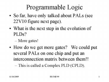
- So far, have only talked about PALs (see 22V10
figure next page). - What is the next step in the evolution of PLDs?
- More gates!
- How do we get more gates? We could put several
PALs on one chip and put an interconnection
matrix between them!! - This is called a Complex PLD (CPLD).
2
22V10 PLD
3
Programmable interconnect matrix.
Cypress CPLD
Each logic block is similar to a 22V10.
4
Any other approaches?
Another approach to building a better PLD is
place a lot of primitive gates on a die, and then
place programmable interconnect between them
5
Field Programmable Gate Arrays
The FPGA approach to arrange primitive logic
elements (logic cells) arrange in rows/columns
with programmable routing between them.
- What constitutes a primitive logic element? Lots
of different choices can be made! Primitive
element must be classified as a complete logic
family. - A primitive gate like a NAND gate
- A 2/1 mux (this happens to be a complete logic
family) - A Lookup table (I.e, 16x1 lookup table can
implement any 4 input logic function). - Often combine one of the above with a DFF to form
the primitive logic element.
6
Other FPGA features
- Besides primitive logic elements and programmable
routing, some FPGA families add other features - Embedded memory
- Many hardware applications need memory for data
storage. Many FPGAs include blocks of RAM for
this purpose - Dedicated logic for carry generation, or other
arithmetic functions - Phase locked loops for clock synchronization,
division, multiplication.
7
Altera Flex 10K FPGA Family
8
Altera Flex 10K FPGA Family (cont)
9
Dedicated memory
10
16 x1 LUT
DFF
11
(No Transcript)
12
Emedded Array Block
- Memory block, Can be configured
- 256 x 8, 512 x 4, 1024 x 2, 2048 x 1
13
Issues in FPGA Technologies
- Complexity of Logic Element
- How many inputs/outputs for the logic element?
- Does the basic logic element contain a FF? What
type? - Interconnect
- How fast is it? Does it offer high speed paths
that cross the chip? How many of these? - Can I have on-chip tri-state busses?
- How routable is the design? If 95 of the logic
elements are used, can I route the design? - More routing means more routability, but less
room for logic elements
14
Issues in FPGA Technologies (cont)
- Macro elements
- Are there SRAM blocks? Is the SRAM dual ported?
- Is there fast adder support (i.e. fast carry
chains?) - Is there fast logic support (i.e. cascade chains)
- What other types of macro blocks are available
(fast decoders? register files? ) - Clock support
- How many global clocks can I have?
- Are there any on-chip Phase Logic Loops (PLLs) or
Delay Locked Loops (DLLs) for clock
synchronization, clock multiplication?
15
Issues in FPGA Technologies (cont)
- What type of IO support do I have?
- TTL, CMOS are a given
- Support for mixed 5V, 3.3v IOs?
- 3.3 v internal, but 5V tolerant inputs?
- Support for new low voltage signaling standards?
- GTL, GTL (Gunning Tranceiver Logic) - used on
Pentium II - HSTL - High Speed Transceiver Logic
- SSTL - Stub Series-Terminate Logic
- USB - IO used for Universal Serial Bus
(differential signaling) - AGP - IO used for Advanced Graphics Port
- Maximum number of IO? Package types?
- Ball Grid Array (BGA) for high density IO
16
Altera FPGA Family Summaries
- Altera Flex10K/10KE
- LEs (Logic elements) have 4-input LUTS (look-up
tables) 1 FF - Fast Carry Chain between LEs, Cascade chain for
logic operations - Large blocks of SRAM available as well
- Altera Max7000/Max7000A
- EEPROM based, very fast (Tpd 7.5 ns)
- Basically a PLD architecture with programmable
interconnect. - Max 7000A family is 3.3 v
17
Xilinx FPGA Family Summaries
- Virtex Family
- SRAM Based
- Largest device has 1M gates
- Configurable Logic Blocks (CLBs) have two 4-input
LUTS, 2 DFFs - Four onboard Delay Locked Loops (DLLs) for clock
synchronization - Dedicated RAM blocks (LUTs can also function as
RAM). - Fast Carry Logic
- XC4000 Family
- Previous version of Virtex
- No DLLs, No dedicated RAM blocks
18
Actel FPGA Family Summaries
- MXDS Family
- Fine grain Logic Elements that contain Mux logic
DFF - Embedded Dual Port SRAM
- One Time Programmable (OTP) - means that no
configuration loading on powerup, no external
serial ROM - AntiFuse technology for programming (AntiFuse
means that you program the fuse to make the
connection). - Fast (Tpd 7.5 ns)
- Low density compared to Altera, Xilinx - maximum
number of gates is 36,000
19
Cypress CPLDs
- Ultra37000 Family
- 32 to 512 Macrocells
- Fast (Tpd 5 to 10ns depending on number of
macrocells) - Very good routing resources for a CPLD
Recommended
CrystalGraphics Presentations


