
Si Chip Electrical Contact PowerPoint PPT Presentation
1 / 18
Title: Si Chip Electrical Contact
1
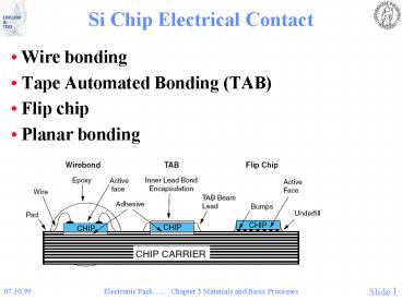
Si Chip Electrical Contact
- Wire bonding
- Tape Automated Bonding (TAB)
- Flip chip
- Planar bonding
2
Wire Bonding
- Ultrasonic
- Thermo-compression
- Thermosonic
- Geometry Types
- Ball - wedgeShown in illustration
- Wedge - wedge
3
Wire Bonding
From Small Precision Tools
4
(No Transcript)
5
Tape Automated Bonding (TAB)
- Fig. 3.26 A picture of a TAB film with the Cu
pattern, as well as the holes in the film for
excising the circuits, and the sprocket holes for
moving the film during processing.
6
Tape Automated Bonding (TAB)
- Interconnection by metallized flexible polymer
tape
7
Tape Automated Bonding (TAB)
- Connection made in two steps
- Inner Lead Bonding
- Connecting tape to chip
- Outer Lead Bonding
- Connecting tape to substrate
- Connection made by thermocompression
8
TAB, continued
- Standard process
- Fabrication of gold bumps (Fig. 3.28)
- Deposition of contact/barrier metals
- Photolithography
- Electroplating
- Strip and etch barrier metals
9
TAB, continued
- Fig. 3.27 The main steps in TAB processing.
10
Advantages of TAB
- High packaging density
- Can contact chips with gt1000 I/O
- Excellent electrical properties (high frequency)
- Robust mounting
- Pre-testable (contrary to COB)
- Gold bumps give hermetic seal to chip
- Gang bonding gives high yield, is less time
consuming than wirebonding - TAB film can be used as daughter board
11
Disadvantages of TAB
- Non-standard wafer processes
- Special custom design film for chip
- Needs special machine/tool for OLB
- Demanding repair
- Low availability of std. chips and TAB service
- Little standardization
12
Flip chip
- Active face of chip is flipped towards substrate
- Substrate pads are identical to chip pads
- Area array connections possible
- All connections done simultaneously
- Smallest possible footprint (11)
- Short interconnections
- Low inductance and resistance
- Excellent electrical properties
- Little flexibility
- Change of chip pad configuration implies redesign
of substrate - Small, but increasing amount of interconnections
are flip chip - To be dealt with in much more detail
13
Flip Chip, history
- Introduced by IBM 1962
- Flip chip has been used for decades, but with
little impact - Wire bonding is far more common
- Flip chip technology has not been considered
mature - The industrial infrastructure has been small
- The market share of flip chip connections is
believed to increase significantly - Wire bonding will remain dominating for many
years - Flip chip especially for advanced packaging
14
Flip Chip consists of
- Chip
- Si, GaAs, etc.
- Substrate
- Ceramic, organic, dielectic-covered metal,
silicon, etc. - Interconnection system
- Metallization on chip and substrate pads
- Chip (or substrate) bumps
- Bonding material
- Underfill encapsulant
15
Different Flip Chip technologies
- Flip chip is not standardized!
From C. Lee, ESTC 2006, Dresden
16
Flip Chip, continued
- Advantages
- Highest packing density
- Excellent hi freq. properties
- Up to 10 000 I/O
- Disadvantages
- Very difficult placement and reliable
solder/cleaning - Lack of thermal flexibility
17
Planar Bonding with Adaptive Routing
- Fig. 3.32 Planar bonding with laser-assisted
adaptive conductor routing. The top two figures
a) and b) show a substrate cross section with
details of the mounting of the chip in an etched
through-hole. Figure c) shows the conductor
layers and polyimide insulation on top of the
substrate. The bottom figures show an exploded
view of all the layers.
18
End of Chapter 3 Materials and Basic Processes
- Important issues
- Materials
- Distinguish between metals, ceramics, glasses and
plastics - Important mechanical and thermal parameters like
modulus of eleasticity, thermal expansion
coefficient and thermal conductivity. - Important electrical parameters like dielectric
constant and resistivity or conductivity - Have a basic understand of the importance and
value of the most important materials parameter,
and why they are important for the use of the
specific material in specific applications. - For instance knowing the electrical conductivity
of copper or thermal conductivity of epoxy within
an accuracy of 25 - Basic processes
- Lithographics, screen and stencil printing,
etching, plating, vacuum deposition, sputtering,
soldering, gluing, wire bonding, TAB, and flip
chip - Other basic processes described in other
chapters, like surface mount technology - Questions and discussions?
Recommended
