
Photoresist Industry PowerPoint PPT Presentations
All Time
Recommended

The Photoresist And Photoresist Ancillaries Market research report analysis from recent past with an eye on coming years in this report that also offers projections Photoresist And Photoresist Ancillaries industry targeted at helping in business decisions.
| PowerPoint PPT presentation | free to download

Photoresist And Photoresist Ancillaries Market
| PowerPoint PPT presentation | free to download

The global photoresist and photoresist ancillaries market size grew from $3.54 billion in 2022 to $3.88 billion in 2023 at a compound annual growth rate (CAGR) of 9.5%.
| PowerPoint PPT presentation | free to download

2014 Deep Research Report on Global LCD Photoresists Industry @ http://www.reportsnreports.com/reports/298088-2014-deep-research-report-on-global-lcd-photoresists-industry.html .
| PowerPoint PPT presentation | free to download

The Global Photoresist Chemicals Industry report gives a comprehensive account of the Global Photoresist Chemicals market. Details such as the size, key players, segmentation, SWOT analysis, most influential trends, and business environment of the market are mentioned in this report. Furthermore, this report features tables and figures that render a clear perspective of the Photoresist Chemicals market. Get Complete Report with TOC : http://www.qyresearchgroup.com/market-analysis/global-photoresist-chemicals-industry-2015-market-research-report.html
| PowerPoint PPT presentation | free to download

The Slitting machine test run and bring into production. 2004.01 ... Contact Person:Elisa Guo. Eternal Photoresist Material Industry (Kunshan) Co., Ltd. ...
| PowerPoint PPT presentation | free to view

See Full Report @ https://goo.gl/YOtHpz. The statistical analysis of the Photoresist Market report depicts the global and Chinese total market of Photoresist Industry including capacity, production, production value, cost/profit, supply/demand and Chinese import/export. The report also estimates 2016-2021 market development trends of Photoresist Market. Photoresist Market Research Report 2016 provides an in-depth study of Global and Chinese Economic Impact on Photoresist Industry. Reports cover the brief description about Global and Chinese Macroeconomic Trends, Development and Analysis. Sample Copy of Report Available @ https://goo.gl/iYnzkj
| PowerPoint PPT presentation | free to download

Download Free Research Report PDF : http://bit.ly/2mpO1kg #Photoresist #MarketAnalysis Photoresist market was valued at USD XX million globally in 2018 and is forecasted to reach USD XX million by 2024, with a CAGR of xx% during the 2018-2024. Full report Url : http://bit.ly/2lX9Szg
| PowerPoint PPT presentation | free to download

The Global And China Photoresist Industry 2017 Market Research Report is a professional and in-depth study on the current state of the Photoresist industry.
| PowerPoint PPT presentation | free to download

Title: Industrial Organic Chemistry Author: JJ Lin Last modified by: jjlin Created Date: 8/19/2000 1:35:04 AM Document presentation format:
| PowerPoint PPT presentation | free to download

The Global And China ArF Immersion Photoresist Industry 2017 Market Research Report is a professional and in-depth study on the current state of the ArF Immersion Photoresist industry.
| PowerPoint PPT presentation | free to download

The 'Global and Chinese Photoresist Industry, 2010-2020 Market Research Report' is a professional and in-depth study on the current state of the global Photoresist industry with a focus on the Chinese market. The report provides key statistics on the market status of the Photoresist manufacturers and is a valuable source of guidance and direction for companies and individuals interested in the industry.
| PowerPoint PPT presentation | free to download

Big Market Research: “Photoresist Market 2019“Size, Share, Industry Trends, Demand, Insights, Analysis, Research, Report, Opportunities, Company Profiles, Forecast
| PowerPoint PPT presentation | free to download

IN MANY LOCATIONS FLUORIDE WASTEWATER DISCHARGE LIMITS ARE ESTABLISHED BY REGULATORY AGENCIES. ... SEGREGATION OF CONCENTRATED FLUORIDE PROCESS DISCHARGES AND ...
| PowerPoint PPT presentation | free to view

Chinese PCB Photoresist Market report available @ http://www.reportsnreports.com/reports/797653-global-and-chinese-pcb-photoresist-industry-2016-market-research-report.html . The report discusses about the basic overview of the industry including its definition, applications and manufacturing technology. Report also explores the international and Chinese major industry players in detail.
| PowerPoint PPT presentation | free to download

Download Free Research Report PDF: http://bit.ly/2qyPFSQ #PhotoresistChemicalsMarket #MarketAnalysis According to this study, over the next five years the Photoresist Chemicals market will register a 4.8% CAGR in terms of revenue, the global market size will reach US$ 3787.2 million by 2024, from US$ 2998.3 million in 2019. Full Report Url: http://bit.ly/2CmCVBh
| PowerPoint PPT presentation | free to download

Download Free Research Report PDF : https://bit.ly/2ZGtbwO A Photoresist Chemicals is a light-sensitive material used in several processes, such as photolithography and photoengraving, to form a patterned coating on a surface. This process is crucial in the electronic industry. Free Research Report PDF: https://bit.ly/2YW6AMj
| PowerPoint PPT presentation | free to download

AGENDA Definition of Photoresist and Types Photoresist Raw Materials and Chemistry Overview of Types Photoresist Process ... IRRADIATION ETCHING PROCESS ...
| PowerPoint PPT presentation | free to download

DecisionDatabases.com adds a report on Global USB Industry 2015 Market Research Report. This research study is segmented on the bases of applications, technology and geography.
| PowerPoint PPT presentation | free to download

Photoresist stripping equipment is used to remove the residuals of photoresists from silicon wafer after it is etched during the semiconductor chip fabrication process. The equipment plays an important role in the chip fabrication process in ensuring that the silicon wafers are free from impurities.
| PowerPoint PPT presentation | free to download

This report was a professional and depth research report on Global Phosphate industry that you would know the world's major regional market conditions of Phosphate industry, the main region including North American, Europe and Asia etc, and the main country including United States ,Germany ,Japan and China etc.
| PowerPoint PPT presentation | free to download

Title: Slide 1 Author: Chuck Fraust Last modified by: sfharper Created Date: 4/6/2004 9:13:43 PM Document presentation format: On-screen Show Company
| PowerPoint PPT presentation | free to download

The World Leader in High-Performance Signal Processing Solutions ... Hazardous wastes are generated from the many types of semiconductor manufacturing processes. ...
| PowerPoint PPT presentation | free to view

Electronic Chemicals & Materials Market is a growing market that deals with production of chemicals and materials that are useful for electronics. These chemicals and materials are used in the structuring and functioning of electronics.
| PowerPoint PPT presentation | free to download

Potential Industrial Application of the One Atmosphere Uniform Glow discharge Plasma(OAUGDPTM) ... One atmosphere, uniform glow discharge plasma. OAUGDPTM setup ...
| PowerPoint PPT presentation | free to view

Actel FPGA (Field Programmable Gate Array) Presentation to NASA and Industry September 22, 2004 Aerospace Actel Team Team Lead: Larry Harzstark Analysis of Boeing ...
| PowerPoint PPT presentation | free to view

Dielectric etching equipment are the specialised equipment which are used in the semiconductor industry for the specific purpose of etching dielectric material during the manufacturing process of a semiconductor. Dielectric etching process refers to an anisotropic process which removes various dielectric substances such as silicon nitride, silicon oxide and different overlying photoresist mask. Increasing demand for the high performance electronic gadgets and miniaturization of semiconductor circuits is expected to remain key growth driver for di-electric etching equipment during the period of study.
| PowerPoint PPT presentation | free to download
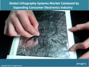
Get more information about the market: https://www.imarcgroup.com/lithography-systems-market According to the latest report by IMARC Group, titled “Lithography Systems Market: Global Industry Trends, Share, Size, Growth, Opportunity and Forecast 2018-2023”, the global lithography systems market reached a value of more than US$ 8.1 Billion in 2017. Lithography, also known as photolithography or semiconductor lithography, is the process of creating the patterns, shapes, locations and dimensions of numerous components in an integrated circuit (IC). These patterns are drawn on silicon wafers using a light sensitive polymer called photoresist. Want more information about this market? Request a free report sample: https://www.imarcgroup.com/request?type=report&id=904&flag=B Contact Us IMARC Group USA: +1-631-791-1145 Email: sales@imarcgroup.com Website: https://www.imarcgroup.com Follow us on twitter : @imarcglobal
| PowerPoint PPT presentation | free to download

Photoresist stripping equipment is used to remove the residuals of photoresists from silicon wafer after it is etched during the semiconductor chip fabrication process. The equipment plays an important role in the chip fabrication process in ensuring that the silicon wafers are free from impurities.The analysts forecast global semiconductor photoresist stripping market to grow at a CAGR of 3.13% during the period 2016-2020.Complete Report available at http://www.sandlerresearch.org/global-semiconductor-photoresist-stripping-market-2016-2020.html.

Suggested Topics. Photoresist for 193 nm lithography. Photoresist for EUV lithography ... Polyimide for dielectric passivation applications. BCB for ...
| PowerPoint PPT presentation | free to view

2015 Deep Research Report on Global Plate-fin Heat Exchanger Industry http://www.deepresearchreports.com/112623.html
| PowerPoint PPT presentation | free to download

[129 Pages] Electronic Grade Sulfuric Acid Market research report categorizes the global market by End-Use Industry (Pharmaceutical & Semiconductor), Grade (PPB & PPT), by Geography
| PowerPoint PPT presentation | free to download

Chemical milling or industrial etching is the subtractive manufacturing process of using baths of temperature-regulated etching chemicals to remove material to create an object with the desired shape.
| PowerPoint PPT presentation | free to download

Title: Brief Silicone Chemistry Review & Silicones for the Skin Care Industry Subject: Ken Kasprzak Author: Sherrie Wegener Last modified by: Wei You
| PowerPoint PPT presentation | free to view

... to define circuit patterns during chip fabrication in the semiconductor industry. ... Tracked trends and steady states for flow, temperature, nitrogen flow, ...
| PowerPoint PPT presentation | free to view

The companies and manufacturers get an understanding into the upstream raw material analysis and downstream demand survey and tracks the impact of market dynamics on industry chain structure
| PowerPoint PPT presentation | free to download

Take a complicated optical system, like a lithographic projection ... Object: reticle or mask. Optics. Aerial Image. Photoresist. Wafer films. Latent Image ...
| PowerPoint PPT presentation | free to view

The market for imaging chemicals photoresists, developers, strippers, and ... In any optical imaging system, the size of the smallest element that can be ...
| PowerPoint PPT presentation | free to download

* The chemical industry has some of the most easily-controllable processes in existence. They are (ideally) pure flow operations Chemical engineers prefer the plug ...
| PowerPoint PPT presentation | free to download

The more complex the system, the more service and higher user costs. Industry Fab. ... Photo Lithography. UV, deep UV. Projection or contact. Micro contact printing ...
| PowerPoint PPT presentation | free to view

Global Electronic Chemicals & Materials Market Size 2019, by Type (Silicon Wafers, PCB Laminate, Photoresist Chemicals, Specialty Gases, Wet Chemicals, and Others), by End-user (Semiconductors, PCB (Printed circuit boards)), by Region and Forecast to 2025
| PowerPoint PPT presentation | free to download

[226 Slides Report] Electronic Chemicals & Materials Market report categorizes the Global market by Types (Silicon Wafer, PCB Laminate, Photoresist, Specialty Gases), Application (Semiconductor & IC, PCB), Forms (Solid, Liquid, Gaseous) & Geography
| PowerPoint PPT presentation | free to download

[226 Slides Report] Electronic Chemicals & Materials Market report categorizes the Global market by Types (Silicon Wafer, PCB Laminate, Photoresist, and Specialty Gases), Application (Semiconductor & IC, PCB), Forms (Solid, Liquid, Gaseous) & Geography
| PowerPoint PPT presentation | free to download

[226 Slides Report] Electronic Chemicals & Materials Market report categorizes the Global market by Types (Silicon Wafer, PCB Laminate, Photoresist, and Specialty Gases), Application (Semiconductor & IC, PCB), Forms (Solid, Liquid, and Gaseous) & Geography
| PowerPoint PPT presentation | free to download

Semiconductor dry strip systems helps in removing photoresist or other residues from a wafer during each step of film deposition or diffusion processing during semiconductor manufacturing process. Globally increasing usage and consumption of electronic gadgets is expected to remain key growth driver for semiconductor dry strips during the period of study.
| PowerPoint PPT presentation | free to download

In this report, our team offers a comprehensive analysis of Li-ion Battery Seperator market, SWOT analysis of the most prominent players in this landscape. Along with an industrial chain,market statistics in terms of revenue, sales, price, capacity, regional market analysis,segment-wise data,and market forecast information are offered in the full study, etc.
| PowerPoint PPT presentation | free to download

Bharat Book Bureau provides the report on “Technical Textiles Market Forecast 2017 to 2021”, (https://www.bharatbook.com/materials-chemicals-market-research-reports-642321/global-technical-textiles1.html)The report provides the technical textiles industry overview with growth analysis and historical & futuristic cost, revenue, demand and supply data.
| PowerPoint PPT presentation | free to download

Global Photolithography Equipment Market stood at USD 15,904.02 million in 2021 and is forecast to register a CAGR of 16.70% by 2027. The demand for photolithography equipment is primarily drive by the high demand for smaller electronic devices, increasing internet of things penetration and the expansion of the semiconductor industry. Moreover, the factors such as high equipment operational and maintenance cost, limitation for curved surfaces hinder the growth of Global Photolithography Equipment Market. Explore Global Market and Key Players Insights: http://tinyurl.com/yc48fdhb

According to the latest research report by IMARC Group, The India semiconductor materials market size reached US$ 4.5 Billion in 2022. Looking forward, IMARC Group expects the market to reach US$ 6.5 Billion by 2028, exhibiting a growth rate (CAGR) of 6.3% during 2023-2028. More Info:- https://www.imarcgroup.com/india-semiconductor-materials-market
| PowerPoint PPT presentation | free to download

According to the latest research report by IMARC Group, The global semiconductor dry strip systems market size reached US$ 377.8 Million in 2023. Looking forward, IMARC Group expects the market to reach US$ 563.2 Million by 2032, exhibiting a growth rate (CAGR) of 4.4% during 2024-2032. More Info:- https://www.imarcgroup.com/semiconductor-dry-strip-systems-market
| PowerPoint PPT presentation | free to download

PHOTOLITHOGRAPHY Photolithography is the heart of the whole integrated circuit technology. It is the process whereby patterns such as diffusion regions, metal tracks ...
| PowerPoint PPT presentation | free to view

Given a multiple choice test, be able to select the correct answer related to ... dark room. Wafer Conditions Prior to Patterning. Surface conditions include: ...
| PowerPoint PPT presentation | free to view

... for waste reduction, recycling, and buying recycled products ... SIA collaborated with EPA to publish a comprehensive guide to Community Right-to-Know Reporting ...
| PowerPoint PPT presentation | free to view

Burr and Stress Free. Complex Designs. Thin Plates as thin as 0.005'. Dr. Lotfi K. Gaafar 2002 ... Copper (oxygen free, rolled...) Nickel. Steel (carbon, ...
| PowerPoint PPT presentation | free to view

Title: Apresenta o do PowerPoint Author: INFORMATICA - MIC Last modified by: INFORMATICA - MIC Created Date: 11/16/2001 3:36:14 PM Document presentation format
| PowerPoint PPT presentation | free to view

As per Delvens market research analysis, the global electronic chemicals and materials market has reached USD 59.7 billion by 2021 and growing at a CAGR of 6.5% during the forecasting period, 2022-2028.
| PowerPoint PPT presentation | free to download