
Amorphous Silicon PowerPoint PPT Presentations
All Time
Recommended

Department of Physical and Astronomical Sciences, University of Palermo, Via ... Electron paramagnetic resonance features of the E' center. Main resonance line ...
| PowerPoint PPT presentation | free to view

Dopant and Self-Diffusion in Silicon and Silicon Germanium Eugene Haller, Hughes Silvestri, and Chris Liao MS&E, UCB and LBNL FLCC Tutorial 4/18/05
| PowerPoint PPT presentation | free to download

The China Thin Film Amorphous Silicon Solar Cell Market Research Report Forecast 2017-2021 is a valuable source of insightful data for business strategists. It provides the Thin Film Amorphous Silicon Solar Cell industry overview with growth analysis and historical & futuristic cost, revenue, demand and supply data (as applicable).
| PowerPoint PPT presentation | free to download

Device Physics of Nanocrystalline (and Amorphous) Silicon Solar ... Valence Bandtail Width. DEV. Bandtail Parameters. Syracuse 6. Power Density vs. Temperature: ...
| PowerPoint PPT presentation | free to view

Process and Material Properties Of PECVD Boron-Doped Amorphous silicon Film. ... A 2000 Angstrom thick PECVD silicon nitride film was deposited on a glass ...
| PowerPoint PPT presentation | free to view

FLCC Seminar Title: Dopant and Self-Diffusion in Silicon, Germanium and Silicon-Germanium Faculty: E. E. Haller GSRA: Chris Liao Department: MS&E
| PowerPoint PPT presentation | free to download

Short after the development of the first solar cell based on amorphous silicon ... The research is focused now on a mixture of material improvement and engineering ...
| PowerPoint PPT presentation | free to view

This Report provided by GrandResearchStore is about, sales (consumption) of Boat Solar Panels in Europe market, especially in Germany, UK, France, Russia, Italy, Benelux and Spain, focuses on top players in these countries, with sales, price, revenue and market share for each player in these Countries, covering Solbian Energie Alternative Enecom Aurinco AB Kyocera Marlec Engineering
| PowerPoint PPT presentation | free to download

Results and discussion. Conclusions. Experimental details. Materials, ... discussion ... SiO2 group in Palermo. Related papers. G. Buscarino, S. Agnello anf F. ...
| PowerPoint PPT presentation | free to view

Study of Thermal Properties in Zr-Al-Cu-Ni Amorphous Alloy by Adding ... width were prepare by a single roller melt-spinning technique in an argon atmosphere. ...
| PowerPoint PPT presentation | free to download

High Pressure Phase Transformations (HPPT) of Silicon, Germanium, and Silicon ... We have developed a mechanistically-based model to describe the process based on ...
| PowerPoint PPT presentation | free to view

silicon fabricated in insulator and basic steps
| PowerPoint PPT presentation | free to view

Need to extend Moore's Law. Commercial Availability of SOI wafers ... IBIS's commercial SIMOX wafers (3'' 6'') 1987. Novel SOI Devices. Dual gate SOI. ...
| PowerPoint PPT presentation | free to download

Semiconductor Processing Single Crystal Silicon Professor Masoud Agah ECE Department Crystal Structure Solid in crystalline and amorphous forms Crystalline solids ...
| PowerPoint PPT presentation | free to view

Crystalline Versus Amorphous Solids Liquids, upon cooling, tend to crystallize. This means that atoms weakly bound in the liquid in a random-like manner arrange them-
| PowerPoint PPT presentation | free to view

Silicon electrical properties. 5 * The appearance of Band Gap, separating CB and VB * The 6 CB minima are not located at the center of 1st Brillouin zone, INDIRECT GAP
| PowerPoint PPT presentation | free to view

This technology gives us flexibility to freely adjust the deposited layers ... Compact Arrayed Waveguide Grating Demulti-plexers Based on Amorphous Silicon Nanowires ...
| PowerPoint PPT presentation | free to view
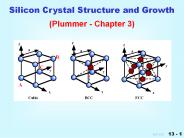
Silicon Crystal Structure and Growth ... mobile electrons tend ... Wafer positioning stage Three-axis piezo substage Figure 7.16 Detector Pinhole ...
| PowerPoint PPT presentation | free to download

Free volume and the glass transition ... Liquid/amorphous g(r), for large r exhibit oscillatory exponential decay. Crystal g(r) does not exhibit an exponential decay ...
| PowerPoint PPT presentation | free to view

Metallic glasses are made by rapid cooling of a metallic liquid such that there ... In the original metallic glasses the required cooling rate was as much as a ...
| PowerPoint PPT presentation | free to view

To separate a thin device layer from the bulk of the wafer. by inserting an electrically insulating layer. Insulator, 0.1 10 um ... Source: Ibis, www.ibis.com ...
| PowerPoint PPT presentation | free to view

1920: fat transplants from abdomen, buttocks. 1940: ... 1950: polyvinyl sponge implants. 1961: Cronin & Gerow (UT) create first silicone implant w/ Dow Corning ...
| PowerPoint PPT presentation | free to view

Silicon wafers have revolutionized the electronics industry and given the digital era a boost. We deal in Silicon Wafer Manufacturing as well as wafer & polishing services. To know more about our products and procedures, visit products/services tab.
| PowerPoint PPT presentation | free to view

Photograph courtesy of Kayex Corp., 300 mm Si ingot. Photo 4.1. EE-452 ... Developmental Specifications for 300-mm Wafer Dimensions and Orientation. Table 4.4 ...
| PowerPoint PPT presentation | free to view

Solar Cell Chapter 7: Manufacturing Silicon Solar Cells Nji Raden Poespawati Department of Electrical Engineering Faculty of Engineering University of Indonesia
| PowerPoint PPT presentation | free to view

Download free PDF Sample: https://bit.ly/2W6ZTHi #AmorphousMetalRibbons #MarketAnalysis The probable scenario is expected to grow by a xx% in 2020 and the revenue will be xx in 2020 from US$ 705.3 million in 2019. The market size of Amorphous Metal Ribbons 3900 will reach xx in 2026, with a CAGR of xx% from 2020 to 2026.
| PowerPoint PPT presentation | free to download

Tom Knight. Radhika Nagpal. Randy Rettberg. Erik Rauch. Gerald ... automata we are moving much more in the dark than nature appears to be with its organisms. ...
| PowerPoint PPT presentation | free to view

In simple words, Silicon wafer reclaim is the method of restoring a used wafer to its original state at a lower cost. This is unquestionably a more cost-effective choice than purchasing fresh wafers.
| PowerPoint PPT presentation | free to download

Silicon Thin Films Solar Cell: Its Recent Development
| PowerPoint PPT presentation | free to view

Solar Cell Chapter 7: Manufacturing Silicon Solar Cells Nji Raden Poespawati Department of Electrical Engineering Faculty of Engineering University of Indonesia
| PowerPoint PPT presentation | free to view

The nanostructure of silicon thin films for solar cells
| PowerPoint PPT presentation | free to view

... a Philips PW-1710 automated diffractometer using a Cu tube operated ... Silicon powder was used as an external standard for calibration of diffractometer. ...
| PowerPoint PPT presentation | free to download

The importance of silicon and its compound in daily life 7S04 Chan Siu Yee 7S08 Chiu Yin Ling Introduction of silicon The 2nd most abundant element in the universe ...
| PowerPoint PPT presentation | free to view

Amorphous Silicon on Windows. Stationary. Sanyo HIT. Alt 1 ... 258 sq. ft amorphous silicon window (5% conversion) 1182.4 kWh available per day for windows ...
| PowerPoint PPT presentation | free to download

... formation of metal oxide and nitride thin films chemical vapour deposition chemical vapour deposition diapositiva 7 metal organic chemical vapor deposition, ...
| PowerPoint PPT presentation | free to view

Introduction Amorphous arrangement of atoms means that there is a possibility that multiple Si atoms will be connected Thin wires of Si within SiO2 layer ...
| PowerPoint PPT presentation | free to download

Radiation Hardened Electronic Devices and Components Market: By Components (Memory, Power ICs, Others) By Materials (Silicon Carbide, Gallium Nitride, Hydrogenated Amorphous Silicon) Verticals (Industrial, Consumer Electronics, Others)-Forecast (2018-2023)
| PowerPoint PPT presentation | free to download

e-MRS/IUMRS 2006 Spring Meeting: May 29-June 02, 2006, Nice, France ... nc-Si films present (feeble) emissions in both the IR and visible range ...
| PowerPoint PPT presentation | free to view

... good stability Sputtering techniques (Ion beam, or magnetron) ... fluence and pulse duration The particulate content decreases with the wavelength PLD ...
| PowerPoint PPT presentation | free to download

High anneal temperatures used to study oxygen related Donors. ... Larger donor density in hot cut film from 400-450 C exfoliation anneal. ...
| PowerPoint PPT presentation | free to view

Sawtooth shaped p strips induce potential gutters. The depth of the potential gutters depends: ... Confining potential gutters are disturbed. Conclusion: ...
| PowerPoint PPT presentation | free to download

... In2O3 on clean 0.38mm thick 4.4mm*4.4mm Silicon substrate. High Tc at high resistance 2.3K @ 7kW. Current films are 30nm thick morphologically ...
| PowerPoint PPT presentation | free to view

Poly-silicon shortage in 2006. Primary Limiting factors. Manufacturing costs ... Energy Conversion Devices (Amorphous Silicon Alloy) ...
| PowerPoint PPT presentation | free to view

Introduction Amorphous arrangement of atoms means that there is a possibility that multiple Si atoms will be connected Thin wires of Si within SiO2 layer ...
| PowerPoint PPT presentation | free to view

I've written a popular science book The Physics of Superheroes. Amorphous Silicon Solar Cells ... Physics is a quantitative science, so units and accuracy are ...
| PowerPoint PPT presentation | free to view

Solar Cell Films Market (Type - Amorphous Silicon, Cadmium Telluride, and Copper Indium Gallium Selenide; End User - Residential, Commercial, and Industrial) - Global Industry Analysis, Size, Share, Growth Trends, and Forecast 2015 - 2023
| PowerPoint PPT presentation | free to download

2. Reactive ion etching for backside of the substrate. Ar CF4. 3. Sample ... The backside layer thickness dependence can help the estimation of the substrate ...
| PowerPoint PPT presentation | free to view

Challenging the Identification of Silicon Nitride Dust in Extreme Carbon Stars ... Leech K., et al., 2003, The ISO Handbook, Volume V - SWS - The Short Wavelength ...
| PowerPoint PPT presentation | free to view

Immediate results - X-Ray images displayed in 5 seconds of less ... Model Varian PaxScan 2520E. Receptor Type Amorphous Silicon. Conversion Screens CsI ...
| PowerPoint PPT presentation | free to view

... calculated frequency shifts (lines) for fully unstrained SiGe films (Eqs. ... shift of the Si Si,Si Ge and Ge Ge phonon modes for the unstrained Si1xGex layer ...
| PowerPoint PPT presentation | free to view

... cost-effective and available commercially, thanks to two technological advances: ... Time-of-Flight (TOF) TOF transient photoconductivity technique: ...
| PowerPoint PPT presentation | free to download

Monolithic Si pixels early prototyping ... Hybrid vs. Monolithic. Sandwich of a sensor substrate bump bonded to the readout chip ...
| PowerPoint PPT presentation | free to view

To create the commercial plastic electronics industry and lead a revolution in ... The performance of organic semiconductors is approaching that of amorphous silicon ...
| PowerPoint PPT presentation | free to view

The collection enhancement and the Purcell enhancement were estimated at 14 and ... We also estimate the average Purcell factor using the measured Q factor, ...
| PowerPoint PPT presentation | free to view

... and chemicals Solar energy production of amorphous silicon and polymer solar cells nano-structured 3D solar cells ... for solar cell production UT/CTW ...
| PowerPoint PPT presentation | free to view

Download Free Research Report PDF @ http://bit.ly/2kquLm1 #SilicaFume #MarketAnalysis Silica fume is a product that's formed by reducing high-purity quartz with coal during the production of silicon or ferrosilicon alloy. Silica fume is composed primarily of pure silica in a non-crystalline form. It consists of amorphous silicon dioxide in high concentration (more than 9Q%) and is a fine spherical particle. Full Report Url - http://bit.ly/2lQOBai
| PowerPoint PPT presentation | free to download