
Programmable Array Logic (PAL) - PowerPoint PPT Presentation
Title:
Programmable Array Logic (PAL)
Description:
Boolean function must be simplified to fit into each section. Unlike, PLA product term cannot be shared among two or more OR gates ... Verilog HDL. Exercise ... – PowerPoint PPT presentation
Number of Views:2837
Avg rating:3.0/5.0
Title: Programmable Array Logic (PAL)
1
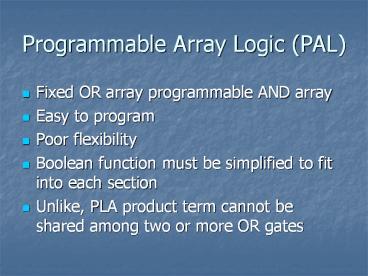
Programmable Array Logic (PAL)
- Fixed OR array programmable AND array
- Easy to program
- Poor flexibility
- Boolean function must be simplified to fit into
each section - Unlike, PLA product term cannot be shared among
two or more OR gates
2
PAL with 4-input 4-output 3-wide AND-OR structure
3
Use PAL to design combinational logic circuit
- Boolean function
- simplified
- PAL programming table is similar to that of PLA
except that only inputs of AND gates need to be
programmed.
4
PAL programming table
5
Fuse map of PAL
6
Sequential Programmable Device
- Digital systems are designed using flip-flop and
gates - PLD contains only gates
- Sequential Programmable Device include both
flip-flop and gates - Three major types
- 1. Sequential (simple) programmable logic device
(SPLD) - 2. Sequential programmable logic device (CPLD)
- 3. Field programmable gate array (FPGA)
7
SPLD
- SPLD AND-OR array F.F. (See Fig. 7-18)
- Output can be taken from OR gates or output of
F.F. - F.F. can be D or JK
- Each section is called macrocell include
sum-of-product combinational logic and a F.F. - Typically include 8-10 macrocell in a chip (IC)
8
SPLD
9
Field-programmable logic sequential (FPLS)
- First programmable device developed to support
sequential circuits - PLA several F.F. (programmable to D or JK)
- Did not succeed commercially because it has to
many programmable connection
10
Complex PLD (CPLD)
- Collection of several individual PLD
- Fig. 7-20 shows a general configuration of CPLD
- PLD is interconnected through programmable switch
matrix - I/O blocks provide the connection to IC pin
- Each I/O is driven by 3-state buffer and can be
programmed to act as input or output - The programmable switch matrix receives input
from I/O block and directs it to the individual
macrocell
11
CPLD
12
Field Programmable Gate Array (FPGA)
- VLSI
- Elementary element is logic block
- Consists hundreds or thousands logic block
- Logic block consists of look-up table,
multiplexers, gates and F.F. - Look-up table is a truth table stored in a SRAM
and provides the combinational function for the
logic block - Remember that PAL or PLA is used for macrocell in
CPLD
13
FPGA
- Use RAM instead of ROM
- Advantage programmable
- Disadvantage volatile
- PLD, CPLD, FPGA requires CAD
- Schematic
- HDL
- VHDL
- Verilog HDL
14
Exercise
- 7-1, 7-2, 7-4, 7-6, 7-8, 7-9, 7-15, 7-17, 7-18,
7-19, 7-20, 7-21, 7-24, 7-25