CMOS fabrication Process Overview - PowerPoint PPT Presentation
1 / 10
Title:
CMOS fabrication Process Overview
Description:
Composite layout and cross-section view of n-well CMOS device ... CMOS process, the doping density of the well region is typically about one order ... – PowerPoint PPT presentation
Number of Views:2574
Avg rating:3.0/5.0
Title: CMOS fabrication Process Overview
1
Complementary MOS fabrication
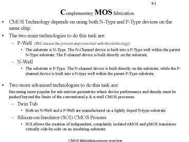
- CMOS Technology depends on using both N-Type and
P-Type devices on the same chip. - The two main technologies to do this task are
- P-Well (Will discuss the process steps involved
with this technology) - The substrate is N-Type. The N-Channel device is
built into a P-Type well within the parent N-Type
substrate. The P-channel device is built directly
on the substrate. - N-Well
- The substrate is P-Type. The N-channel device is
built directly on the substrate, while the
P-channel device is built into a N-type well
within the parent P-Type substrate. - Two more advanced technologies to do this task
are - Becoming more popular for sub-micron geometries
where device performance and density must be
pushed beyond the limits of the conventional p
n-well CMOS processes. - Twin Tub
- Both an N-Well and a P-Well are manufactured on a
lightly doped N-type substrate. - Silicon-on-Insulator (SOI) CMOS Process
- SOI allows the creation of independent,
completely isolated nMOS and pMOS transistors
virtually side-by-side on an insulating
substrate.
2
P-well on N-substrate
- Steps
- N-type substrate
- Oxidation, and mask (MASK 1) to create P-well
(4-5?m deep) - P-well doping
- P-well acts as substrate for nMOS devices.
- The two areas are electrically isolated using
thick field oxide (and often - isolation implants not shown here)
SiO2
P-well
3
Polysilicon Gate Formation
- Steps
- Remove p-well definition oxide
- Grow thick field oxide
- Pattern (MASK 2) to expose nMOS and pMOS active
regions - Grow thin layer of SiO2 (0.1?m) gate oxide, over
the entire chip surface - Deposit polysilicon on top of gate oxide to form
gate structure - Pattern poly on gate oxide (MASK 3)
4
nMOS P Source/Drain difusion self-aligned to
Poly gate
Implant P nMOS S/D regions (MASK 4)
P implant/diffusion
P mask
Thick field oxide
P
N-type substrate
5
pMOS N Source/Drain difusion self-aligned to
Poly gate
Implant N pMOS S/D regions (MASK 5 often the
inverse of MASK 4)
N implant/diffusion
N mask
P
N
P
N-type substrate
6
pMOS N Source/Drain difusion, contact holes
metallisation
Oxide and pattern for contact holes (MASK
6) Deposit metal and pattern (MASK 7) Passivation
oxide and pattern bonding pads (MASK 8) P-well
acts as substrate for nMOS devices. Two separate
substrates requires two separate substrate
connections Definition of substrate connection
areas can be included in MASK 4/MASK5
Vout
Vss
N for N-substrate contact)
P (for P-substrate contact)
P
P channel Device
P
N
N channel Device
N-type substrate
7
CMOS N-well process
An N-well process is also widely used
P for P-substrate contact)
Vout
N (for N-substrate contact)
Vss
N-well
N channel Device
N
P
P channel Device
P-type substrate
8
Composite layout and cross-section view of n-well
CMOS device (excludes passivation and patterning
of wire-bonding pads)
9
Twin-Tub (Twin-Well) CMOS Process This
technology provides the basis for separate
optimization of the nMOS and pMOS transistors,
thus making it possible for threshold voltage,
body effect and the channel transconductance of
both types of transistors to be tuned
independently. Generally, the starting material
is a n or p substrate, with a lightly doped
epitaxial layer on top. This epitaxial layer
provides the actual substrate on which the n-well
and the p-well are formed. Since two independent
doping steps are performed for the creation of
the well regions, the dopant concentrations can
be carefully optimized to produce the desired
device characteristics. The Twin-Tub process is
shown below.
In the conventional p n-well CMOS process, the
doping density of the well region is typically
about one order of magnitude higher than the
substrate, which, among other effects, results in
unbalanced drain parasitics. The twin-tub process
avoids this problem.
10
Silicon-on-Insulator (SOI) CMOS Process Rather
than using silicon as the substrate material,
technologists have sought to use an insulating
substrate to improve process characteristics such
as speed and latch-up susceptibility. The SOI
CMOS technology allows the creation of
independent, completely isolated nMOS and pMOS
transistors virtually side-by-side on an
insulating substrate. The main advantages of this
technology are the higher integration density
(because of the absence of well regions),
complete avoidance of the latch-up problem, and
lower parasitic capacitances compared to the
conventional p n-well or twin-tub CMOS
processes. A cross-section of nMOS and pMOS
devices using SOI process is shown below.
The SOI CMOS process is considerably more costly
than the standard p n-well CMOS process. Yet
the improvements of device performance and the
absence of latch-up problems can justify its use,
especially for deep-sub-micron devices.

