
Plasma Arc Lamp Operation - PowerPoint PPT Presentation
1 / 19
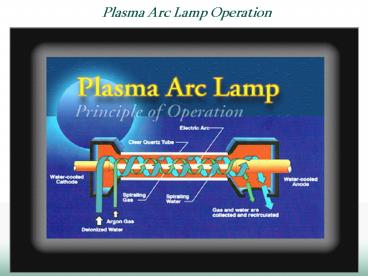
Title: Plasma Arc Lamp Operation
1
Plasma Arc Lamp Operation
2
Properties of the Plasma Radiant Source
- Maximum lamp power 35 MW/m2
- Non-contact heating
- Rapid heating and cooling
- Concentration of heating on surface
- Environment argon, vacuum, air
- Three separate plasma heads 10, 20 and 35 cm
arcs - Power delivery flash mode or scan mode as wide
as 35 cm, presently - Lamp power form 2 to 100 of available radiant
output - Change of power levels less than 20 ms
- Wavelength of radiant output 0.2-1.4 µm
- Wavelength constant and independent of power
level and anode/cathode wear
3
Coating Procedure
SiC (Hexoloy SA)
Plasma Arc Lamp
Flash orscan
Pretreatment
Brush or spray powder (W or Mo)
W or Mo powder
IR processing
Vapor deposited W or Mo
Anneal
Pretreatment Ti vapor deposition W or Mo
vapor deposition Anneal 72 hours (1300 or
1500ºC)
Vapor deposited Ti
SiC
Specimen size 25153 (mm) IR processing
uniform irradiance or scan
4
Effect of IR Processing on Surface Roughness
SiC without coating
IR processing
OM images
W coating
Interface
SiC
10µm
SiC was removed by sublimation of the surface of
the SiC prior to ordering the W powder melt.
Rough interface was formed.
5
Effect of Scan Speed on Coating Surface
IRHW31
IRHW32
IRHW30
IRHW27
Melted W
Melted W
Melted W
Melted W
Crack
Non-melted W
Non-melted W
Scan speed 11.0 mm/sec
10.5 mm/sec
10.0 mm/sec
5.0 mm/sec
5mm
Hexoloy SiC W (no pretreatment), Lamp power
23.5 MW/m2 Melting point of tungsten 3370 ºC
6
Effect of Scan Speed on Coating Microstructure
IRHW31
Melted W
W coating
Non-melted W
5mm
SiC
Scan speed 11.0 mm/sec
Cross sectional SEM image in middle region
Hexoloy SiC W (no pretreatment), Lamp power
23.5 MW/m2
7
Effect of Scan Speed on Coating Microstructure
IRHW32
Melted W
W coating
Non-melted W
5mm
Scan speed 10.5 mm/sec
SiC
Cross sectional SEM image in middle region
Hexoloy SiC W (no pretreatment), Lamp power
23.5 MW/m2
8
Effect of Scan Speed on Coating Microstructure
IRHW30
W coating
Melted W
5mm
Scan speed 10 mm/sec
SiC
Cross sectional SEM image in middle region
Hexoloy SiC W (no pretreatment), Lamp power
23.5 MW/m2
9
Relationship between Lamp Power and Maximum Scan
Speed to Melt Coating
10
SEM Images of W Coating Processed at 23.5 MW/m2
WC
W coating
SiC
- No thick reaction interlayer
- WC grains adjacent to interface
- Strong interface
Lamp power 2350 W/cm2, 10 mm/sec scan
Back scattering SEM images
11
SEM Images of W Coating Processed at 18.28 MW/m2
WC
W coating
SiC
Lamp power 2350 W/cm2, 10 mm/sec scan
- No thick reaction interlayer
- WC grains adjacent to interface
- Strong interface
- Eutectic structure
WC
Back scattering electron images
12
Effect of Processing Condition onFlexural
Strength of W Coated SiC
Substrate strength
W coating side
Four point flexural test Specimen size 50x4x3
mm Support span 40 mm Loading span 20
mm Crosshead speed 10um/sec
- W coating was not peeled off during flexural test
- Strength of substrate SiC was decreased by IR
processing - Vapor deposition prior to powder coating
prevented degradation of strength slightly
13
EDS Mapping of W Coating (Higher Power, Slower
Scan)
W
Wcoating
C
WC
WSi
SiC
10µm
Back scattering electron image
Si
EDS mappingof W, C, Si?
Hexoloy SiC W (no pretreatment) Lamp power
2350 W/cm2 Scan speed 9mm/sec
14
Effect of Vapor Deposited W and Pre-heating on
Crack Propagation into SiC
W coating
SiC
2350W/cm2(3sec)
VD W2350W/cm2(3sec)
10µm
522W/cm2(20sec)2350W/cm2(3sec)
Vapor deposition of W and pre-heating
significantly reduced cracks within the SiC.
15
SEM Images of W coating Formed by Uniform
Irradiance
With pre-heating 522W/cm2 (20sec) 2350W/cm2
(3sec)
SiW
SiC
W coating
WC
SiC
Back scattering (composition) electron image
SiC and WxSiy grains which were not seen a
coating by scanning method, were seen.
16
Thermal Fatigue Experiment Using IR Processing
Facility
W coated specimen
Cooling table
Rep rate 10Hz Max. flux 23.5MW/m2 (10ms) Min.
flux 5.9MW/m2(90ms) Substrate temp. (bottom)
600 ºC
Substrate material silicon carbide Coating
material tungsten (50µm-thick) Specimen size 50
x 4 x 3 (mm)
17
Effect of Thermal Fatigue on Tungsten Coating
Before experiment
Tungsten coating was not peeled off following
1000 cycle thermal fatigue experiments
After 1000 cycles
Rep rate 10Hz Max. flux 23.5MW/m2 (10ms) Min.
flux 5.9MW/m2(90ms) Cycle 1000 Substrate temp.
(bottom) 600 ºC
18
Summary of IR processing
- Silicon carbide was removed by sublimation of the
surface of the SiC prior to ordering the W powder
melt. Rough interface was formed. - It was found that less reaction time made W
coating porous and too much reaction time break
SiC. The scan speed and processing time were
optimized for each lamp power. - The WxCy grains were formed near interface within
W coating in all specimens. Many round WxCy
grains and eutectic structure were found in the
coating formed at lower power and slower scan
speed, while those were not found in the coating
formed at higher power and faster scan speed. - In uniform irradiance, SiC was broken easily by
IR processing. It was found that vapor deposition
of W and pre-heating significantly reduced cracks
within the SiC. The scanning processing also
reduced the cracks within SiC, since it includes
pre-heating. - Not only W grains adjacent to interface SiC and
WxSiy grains were observed within W coating.
19
Summary of Thermal Fatigue Experiment
- Thermal fatigue experiments were carried out
successfully using IR processing facility.
Preliminary results showed tungsten coating was
stable following the heat load (10Hz, 23.5MW/m2
(10ms), 1000cycles).
Recommended
CrystalGraphics Presentations


