
9 Applications of BJT - PowerPoint PPT Presentation
1 / 37
Title: 9 Applications of BJT
1
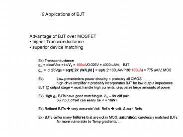
9 Applications of BJT
- Advantage of BJT over MOSFET
- higher Transconductance
- superior device matching
Ex) Transconductance gm dIc/dVbe Ic/VT
100uA/0.025V 4000 uA/V, BJT gm dId/dVgs
sqrt 2k (W/L)Id sqrt( 2100uA/V230100uA)
775 uA/V, MOS Ex) Low-power/micro-power
circuitry probably all CMOS high-drive
amplifier probably incorporates BJT for low
output impedance BJT _at_ output stage must handle
high currents, dissipates large amounts of
power Ex) High gm BJTs have good matching in Vbe
for diff pair 3s input offset can easily be lt
1mV ! Ex) Ratioed BJTs ? very accurate Volt.
Ref.s ? volt. curr. Refs. Ex) BJTs suffer many
failures that are not in MOS saturation,
carelessly matched BJTs far more vulnerable
to Temp gradients,
2
9.1 Power BJT
- Because of high-Ic rolloff (gt1.5uA/um2), emitter
area increases. If to conserve space, then
work at lower beta than small-signal BJTs.
Beta min. acceptable 10 (power NPN can handle
8-15 uA/um2). - Lateral PNP can not achieve more than 250uA/
min.emitter - Small-signal BJT can handle 10 mA, 100 mW
- Power BJTs for gt100mA, gt500mW need special
layout, up to as high as 10A 100W - Most IC power NPN Ilt2A Plt10W
- Power PNP Ilt500mA.
3
Failure of Power NPN
- Emitter debiasing
- thermal runaway
- secondary breakdown
4
(A) Emitter debiasing some Tr may not even
conduct
Ex) suppose Ie 50mA, R 1.2mW each ? total
Volt drop 50mA 1.2mW 100mA 1.2mW 150mA
1.2mW 3.6mV ? DIe/Ie e3.6mV/26mV -1 1.15 -1
15
Metal lead R
5
(A) Emitter debiasing some Tr may not even
conduct
Ex) suppose Ie 50mA, R 1.2mW each ? total
Volt drop 50mA1.2mW 100mA1.2mW
150mA1.2mW 3.6mV ? DIe/Ie e3.6mV/26mV -1
1.15 -1 15
15 morecurrent than Q1 !
Ve1
Metal lead
Ve1-3.6mV
6
- (B) Use Emitter Ballasting R
- to reduce impact of E debiasing
- Insert R at Emitter node
- typically 50-75mV drop at max full rated current
- Ex) 50mA Em. ? 1W R
7
- (B) Use Emitter Ballasting R
- to reduce impact of E debiasing
- Insert R at Emitter node
- typically 50-75mV drop at full rated current
- Ex) 50mA Em. ? 1W R
- Ex) (1) 3.6mV debiasing ? (2) current change in
Ballasting Rs ? (3) change in Emitter terminal
voltage
DVe 1.8mV
DVe -1.8mV
50mA1.8mA
1W
50mA-1.8mA
D -1.8mV
D 1.8mV
8
(No Transcript)
9
Voltage drop should not exceed 5mV
2
Emitter contact
1
? Because exp(5mV/25mV)-1 1.22-1 22
difference between IE1/IE2
DVBE L Rs IE / 2W
Ex) 50mA along the length of 300um (L), 30um (W),
and 12mW/sq (Al, Rs) ? 3001250/230 3mV
acceptable
Emitter Current Flow Direction
10
Thermal Runaway
dVBE/dT - 2 mV/C --- initially starts
with E debiasing
Hot spots conduct more current !
Secondary Breakdown If JE gt Jcrit VCE gt VCEO2
? leads to overheating metallization failure
Example BJT driving inductive load ? vulnerable
to secondary breakdown
? Keep IE lt 8-15uA/um2
11
Layout of Power NPN
Linear-mode PE lt 150uW/um2, IE lt
8uA/um2 Switched-mode less average Power during
operation. IE lt 16uA/um2 Pulsed-mode Large
current during a few 100nS, immune to thermal
runaway ex) Capacitive load like MOS gate
Interdigitated-Emitter NPN oldest style,
higher speed
12
- Two emitter Ballasting Rs
- extremely vulnerable to inter-finger debiasing
must be DVinterfinger lt 5mV - Large of short fingers better than small of
long fingers - compromised finger widths 8-25 um
- Emitter contact as large as possible to reduce
RE
13
- Previous geometry Base metallization
comb-style
- Below is Serpentine-style Base metallization
14
Wide-Emitter Narrow-Contact NPN
- Narrow Emitter Fingers
- Good for high freq. due to low RB
- good for controlling Emitter crowding
- bad for intrafinger debiasing (concentrates
conduction at one end of finger) - ? individually ballasted sections (no one finger
can conduct too much) - ? use wide emitter, narrow contact for similar
effect (distributed network of
ballasting resistors)
15
Christmas-tree Power NPN
- Widely used in Linear-mode app due to resistance
to thermal runaway - Rarely used for switching app
- Emitter central spine triangular prongs
- most conduction in triangular prongs
- Emitter ballasting naturally built in
- At low Ic all parts high Ic only triangular
prongs - best for app that dissipates high power
16
Cruciform-emitter NPN
- Emitter width 75-125um for added ballasting
- Em.contact locations ? distributed 3D ballasting
- wide E/narrow contact Xmas tree
- efficient use of space better than xmas tree
- two drawbacks
- small Em.contacts ? electromigration
- compact size can cause extreme local heating
- Best suited for Switching app.
17
(No Transcript)
18
Power Transistor in Analog BiCMOS
- All forms of Power NPN above plus
Wide-emitter, narrow-contact in BiCMOS
Diffusion masks
Metal-1 masks
19
Saturation (CBJ) detecting limiting
Two examples of PNP to limit saturation
20
Switching NPN Transistor -- example
21
9.2. Matching Bipolar Transistor
Consider two transistors with equal IC. Any
random or systematic difference in IS will lead
to
DVBE VT ln(IS1/IS2)
1 variation in drawn Emitter area ? 1 variation
in IS ? DVBE 26mVln(1.01) 0.26mV
1 mismatch in drawn Emitter area ? 0.26mV Offset
voltage
22
Causes for mismatch are, in its origin, Random or
Systematic variations.
Random the natural fluctuations in Doping
Level (Base) and in Area of EBJ is the main
cause. More minor effects come from recomb. in
EB depletion region and lateral injection
across Base diffusions. These are prop to 1/(A/P)
Systematic i) Trs at a different VBC will
have different IC. (Use Emitter degeneration)
ii) NBL shadow due. (NPN sufficient overlap or
omit PNP no problem) iii) Thermal gradients
causes -2 mV/C. (common-centroid Compactness).
iv) Stress gradients (common-centroid low stress
regions) v) different VCE vi) cross
injection in merged lateral PNP vii) depletion
region intrusion in multiple-Emitter NPN
23
9.2.1 Random Variation
- base doping, Emitter area
- recomb. In E-B deple region
- lateral injection across B-diffusion
3 favored geometries of NPN
- largest A/P ratio
- but by many-sided polygons
- easy accurate
A/P kr sqrt(Ae) kr 0.25 (sq), 0.274 (oct),
0.282 (circle)
24
Random mismatch due to Area Periphery
fluctuation S 1/sqrt(Ae) sqrt ka kr
kp/sqrt(Ae) For Emitter gt 2-3X minimum size,
ignore kp term S sqrt( ka/Ae )
Note Ae too large is not good either due to T
and Stress gradients.
General rule diameter of Emitter of matched
NPN gt 2x lt 10x Of minimum possible diameter
Ex) min. contact width 2um min. overlap of
emitter over contact 1um min. Emitter diameter
1 2 1 4 Emitter diameter 8um 40um
25
- Due to thermal stress gradients, and the
large Collector isolation, it is NOT always
better to use identical unit transistorsconnected
in parallel.
Two styles of multiple NPNs
- common N-tank(C)
- common p-base
- far enough apart between bases or emitters
to prevent carrier flowing between them ?
increase E-to-E spacing Base-overlap-of-E by
1-2 um
26
Emitter Degeneration
- Transfer burden of matching BJTs to matching
Rs ? IF matching Rs is at least as accurate
at matching BJTs - Systematic error due to finite VA for matched
BJTs Ic1/Ic2 1 (DVBC/VA) (VT/VTVd) Vd
degenration voltage - ex) VT26mV, Vd50mV then error decreases by 3x
- Degeneration Rs prop. to 1/Ae
- Ic Rd 50-75mV is sufficient to ensure Rs
determine matching not BJTs, if Ae lies within
- 10 of DESIRED VALUE
27
- IF Rd 250-500mV, THEN Ae of BJT is less
important. - For example 3.41 ratio can be obtained by (3x
Tr 10kW) vs. (1x Tr 34kW)
28
Matched NPN Examples!!
- 9.2.4 Thermal Gradients
- BJTs extremely sensitive to Temp-gradients
dVBE/dT - 2mV/C ? ? dIC/dT 8 / C - Matched BJTs routinely expects - 1mV ? ? dT
- 0.5C - Matched BJTs diff pair, ratioed pair, ratioed
quads
- Ratioed Pair IF Ic1Ic2, THEN DVbe VT
ln(A1/A2) T (VPTAT) - ? or I1 proportional to absolute Temp (IPTAT) in
many op. conditions - ex) A2A181 ? DVbe 54mV ? 1mV mismatch ? 2
error in DVbe
29
- Ratioed Quad for the same Ic, DVbe VT ln(
A1A2/A3A4 ) - ex) two 4X ? 72mV
- ex) two 8X ? 108mV
DVbe (Vbe3Vbe4) (Vbe1Vbe2) VT
ln(Ic3/Is3) ln(Ic4/Is4) VT ln(Ic1/Is1)
ln(Ic2/Is2) VT ln(Is1Is2/Is3Is4)
(Ic3Ic4/Ic1Ic2) VTln(A1A2/A3A4) for same Ic
30
DVbe log (Area Ratio) Mismatch due to Stress
gradient or Thermal gradient sqrt (Area Ratio)
- Therefore,
- Layout of Ratioed Pair or Ratioed QUAD
- SYMMETRY
- COMPACT
31
- Critical matched devices ? Common-centroid
layout - can not completely cancel NONLINEAR thermal
variation ? make it COMPACT !!!
Example
Cross-coupled quad for differential pair
32
Common-centroid example for Ratioed Pair
- Make S2 parallel to Isotherms
33
- Ratioed QUADs
- Layout as if they are a pair of ratioed mirrors
- Example
- Q1 1X Q2 1X Q3 4X Q4 8X
34
Location of Common-centroid Bipolars to minimize
the Stress gradients
- Vbe is affected by Stress Gradient, up to a few
mV of offset - Common centroid layout can remove the Linear
Gradients but nonlinear components may still
be present - Best to place the Matched devices in low stress
area, with the Axis of symmetry, S2, // to
the isobar ensured if S1 // axis of symmetry of
die - at least 250um inside the edge, if possible
- Assuming no heat source in immediate vicinity
35
- Location of Matched Bipolars on dice when Power
device is present - Die aspect ratio of 21 is better than 11 for
larger separation
- Emitter degeneration is beneficial IF BJTs are
near Heat source ! But they must be laid out
carefully.
36
- 9.2.7 Other Systematic Mismatches
- Different VCE IC Is exp(VBE/VT) (1 VCE/VA)
- Example DVCE 1V, VA100V gives DIC/IC 1
- Prevention Use circuit design to operated
matched BJTs at same VCE - ii) Collector efficiency of Lat.PNP results in
different Ic. - caused by
- - Different VCE
- - saturating PNP
- iii) Cross injection in Lat.PNP induce Ic
mismatch - ex) multiple PNPs in common Tank, and one
saturates. - Prevention a) place each Lat.PNP in its own
N-Tank. - b) can use N-bar between PNPs
- iv) EBJ Depletion in vertical NPN ex) Emitters
in the same Base diffusion - gt thinned neutral Base region lead to voltage
drop gt less Emitter current - Prevention incease E-to-E spacing the
base-overlap of E by a few um
37
Fig.9.27B two stage BJT opamp
Fig.9.28 Gilbert Multiplier Core
Recommended
CrystalGraphics Presentations


