
Ultrasonic Coating - PowerPoint PPT Presentation
1 / 41
Title:
Ultrasonic Coating
Description:
... spray coverage with 5 independent wafer sensors WideTrack stationary spray heads are proven for continuous ... Perovskite materials. HTM (PEDOT: PSS, P3HT ... – PowerPoint PPT presentation
Number of Views:174
Avg rating:3.0/5.0
Title: Ultrasonic Coating
1
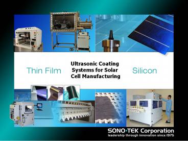
Ultrasonic Coating Systems for Solar Cell
Manufacturing
2
Our History
Sono-Tek Corporation was founded in 1975by Dr.
Harvey L. Berger, Ph.D. Inventor of the
ultrasonic nozzle
The first ultrasonic nozzles were developed for
use in oil burners and subsequently for the
development of liquid fuel burners contracted by
the U.S. Military for use in portable power
generation equipment. Today Sono-Tek offers a
wide selection of precision ultrasonic coating
systems across various industries including
Energy, Defense, Semiconductor, Aerospace,
Medical Devices, Glass Manufacturing, and
Textiles.
3
Common Stock
Sono-Tek became a publicly traded company in
1987. The Companys Common Stock trades in the
over-the-counter market on the OTC Bulletin Board
under the symbol SOTK.
4
Corporate Headquarters
Sono-Teks corporate headquarters is located in
Milton, NY, USA. This facility houses our
factory as well as a full staff, including our
engineering, sales, accounting, manufacturing,
quality control, technical support and shipping
departments. Sono-Tek has a satellite office in
Hong Kong to facilitate sales and service to our
Asian customers. We also have laboratory testing
facilities located in the U.S., Germany, Honk
Kong, Korea, and Taiwan.
5
Ultrasonic Atomization
- When liquid is added to a resonating nozzle,
waves are formed on the atomizing surface - SONO-MATH 101
- ?L((8p?)/(?f2))1/3
- p pi
- ? Surface Tension
- ? Density
- F Frequency of Nozzle
- Increasing the power causes the wave peaks to get
so high that droplets fall off the tips of the
wave. - These droplets have a mathematically definable
size. - SONO-MATH 101
- DN, 0.5.34?L
- Notice also that less of the atomizing surface is
used (for a given flow rate).
6
Industry Expertise
FUEL CELL
ELECTRONICS
SOLAR CELL
MEDICAL
7
Product Line for Solar Cell Manufacturing
- Thin Film Solar Cells
- Deposition of active layers
- Deposition of buffer and/or organic layers
- Deposition of TCO
- Silicon Solar Cells
- SelectaFlux - Fluxing of Solder Bus on
Tabber/Stringer machines - ChemCoat Phosphoric/Boric Doping
- Solar Cell Packing
- 7. Anti-reflection Coatings
8
Thin Film Solar Cells Typical Layering of a Thin
Film Cell
Cells may be comprised of some or all of the
following layers, this is a typical cell in a
substrate configuration.
- GLASS/PROTECTIVE LAYER
- ANTI-REFLECTION LAYER
- TCO
- Buffer Layer / PEDOT (OSC)
- ACTIVE LAYER
- BACK CONTACT
Sono-Tek can coat these layers
9
Product Line for Solar Cell Manufacturing
- Thin Film Solar Cells
- Deposition of active layers
- Deposition of buffer and/or organic layers
- Deposition of TCO
- Silicon Solar Cells
- SelectaFlux - Fluxing of Solder Bus on
Tabber/Stringer machines - ChemCoat Phosphoric/Boric Doping
- Solar Cell Packing
- 7. Anti-reflection Coatings
10
Thin Film Solar Cells Active Layer
- The active layer creates the positive side of the
p-n junction and creates a potential in the thin
film structure. It contains semiconducting
materials which may be one of the following - CIS
- Thickness 1.5 4.5 microns
- CIGS
- Thickness 1.5 - 4.5 microns
- CdTe
- Thickness 2 - 5.5 microns
- CTZS(S)
- Thickness 2 - 5.5 microns
- DSC Thickness 1 3 microns
- Quantum Dots
- Nano-crystal semiconducting dots contain Zn, Pb,
Cd, Se - Perovskites
- Thickness 50nm 1 micron
GLASS/PROTECTIVE LAYER ANTI-REFLECTION LAYER TCO
ACTIVE LAYER BACK CONTACT
Buffer Layer / PEDOT (OSC)
11
Active Layer Coating EquipmentLow to High Volume
Solutions
RD
Low to Mid Volume Production
High Volume Production
12
Thin Film Solar Cells Active Layer
- Alternate deposition methods
- CVD, Sputtering
- Extremely expensive, high initial capital cost
- Batch processing (trending toward inline with new
systems) - In many cases low transfer efficiency as low as
50
13
Product Line for Solar Cell Manufacturing
- Thin Film Solar Cells
- Deposition of active layers
- Deposition of buffer and/or organic layers
- Deposition of TCO
- Silicon Solar Cells
- SelectaFlux - Fluxing of Solder Bus on
Tabber/Stringer machines - ChemCoat Phosphoric/Boric Doping
- Solar Cell Packing
- 7. Anti-reflection Coatings
14
Thin Film Solar Cells Buffer Layer / Use of
Polymers
- CIGS, CDTE, Cells
- Common Buffer Layer
- CdS - Thickness .02 - .05 microns
- ZnS Thickness .02 - .05 microns
- Organic Cells, Perovskite
- Typical Polymers - PCBM, P3HT, P3HD
- PEDOT layer is commonly used with active layers
made of polymers, and acts as an anode, and is
currently used in RD applications - Polymers are often sprayed in inert environment
- Requires very low oxygen levels(lt2 ppm)
- Thickness ( 0.11 0.17 microns)
- Temperature 25 - 75ºC
- Annealed at low temperatures(150 250ºC)
- Mixed with solvents
- Chlorobenzene
- P-Xylene
GLASS/PROTECTIVE LAYER ANTI-REFLECTION LAYER TCO
ACTIVE LAYER BACK CONTACT
Buffer Layer / PEDOT (OSC)
15
Thin Film Solar CellsDSC Organic Solar Cells
Layers
- TCO layers can be created with ultrasonic spray
pyrolysis. - Cathode layer Platinum is most efficient but
high , graphite less expensive and less
efficient. - Electrolyte usually applied in gel form. Needs
to be diluted to be sprayed with ultrasonics. - Dye Usually dip coated but can be applied with
ultrasonic spray. - Compact oxide can be sprayed with ultrasonics,
then heated. - Glass is often purchased with TCO layer already
applied.
16
Thin Film Solar CellsPerovskite Solar Cells
Layers
- Sono-Tek ultrasonic nozzles can be used to spray
the following layers - TCO (CNT, Graphene, Silver Nanowires, ITO FTO
through spray pyrolysis. - Perovskite materials.
- HTM (PEDOT PSS, P3HT)
- Nano-Metals (Nano-Gold, Silver Nanowires)
17
Thin Film Solar Cells ExactaCoat Inert
Commonly used for Organic Solar Cell
Manufacturing Built for continuous operation with
constant positive pressure environment using
Nitrogen, Argon or Helium
- lt1 ppm H2O and O2 inert gas
- Continuous recirculation and on-line monitoring
of O2 and moisture content - Hepa gas flow filters at chamber inlet and outlet
- 36 D x 48 W x 36 H chamber
- Large antechamber - 38 cm (15) OD and mini
antechamber - 15 cm (6) OD - 400 mm x 400 mm x 100 mm
- (15.75 x 15.75 x 3.94) XYZ range of motion
- Includes Windows-based (programming) software
with image import - Nozzles can be easily interchanged to produce
varying spray patterns ranging from 0.080 to 3
(2 - 76 mm) wide
18
Product Line for Solar Cell Manufacturing
- Thin Film Solar Cells
- Deposition of active layers
- Deposition of buffer and/or organic layers
- Deposition of TCO
- Silicon Solar Cells
- SelectaFlux - Fluxing of Solder Bus on
Tabber/Stringer machines - ChemCoat Phosphoric/Boric Doping
- Solar Cell Packing
- 7. Anti-reflection Coatings
19
Thin Film Solar Cells TCO/Contact Grid
- TCO (Transparent Conductive Oxide) consists of
metals dissolved in solution having high
conductive and transparent properties. It acts
as the front contact to the device and is needed
to reduce the series resistance of the device.
Sometimes applied at high temperatures in
pyrolysis reaction. Also, they often require
high temperature annealing at 500 600 degrees
C. - ITO
- Can increase conductivity of ITO in 2 ways
- Increasing heat - Increasing the temperature of
the substrate during the coating process has
indicated an increase in conductivity - Increasing thickness of ITO layer ( 0.04
microns) - Problems
- As thickness increases, cracking is more
susceptible - ZnO ( 0.2 - 0.5 microns)
- Doped with Ga, Al, In
- Structure and morphological properties same for
Ga, Al and In - Optical properties much better for In (smoother)
than for Ga or Al - ZnO has the highest piezoactivity compared to
other TCOs - CdO
- Doped with In, Sn, F
- F is preferred because of low cost and is less
hazardous - SnO2 (Commonly SnO2 F or FTO)
GLASS/PROTECTIVE LAYER ANTI-REFLECTION LAYER TCO
ACTIVE LAYER BACK CONTACT
Buffer Layer / PEDOT (OSC)
20
Spray Pyrolysis Applications
- Definition of Spray Prolysis - A process in which
thin film is deposited by spraying solution onto
a heated surface, where constituents react to
form a chemical compound - One Major Glass Manufacturer 6 million m2/yr
doing spray pyrolysis on float glass line. 600
700 degrees C. - ExactaCoat for TCO Duplicates this process on a
smaller scale. Can be scaled up to much larger
process, i.e. float glass line.
21
Thin Film Solar Cells ExactaCoat for TCO RD
System
- Fully Enclosed XYZ Motion System for Ultrasonic
Spray Pyrolysis, depositing TCO layers in RD
scale spray applications. - Precise substrate uniformity with repeatability
down to /-2 - Compact benchtop design that favors portability
- 400 mm x 400 mm x 100 mm (15.75 x 15.75 x
3.94) range of motion - PathMaster Windows-based programming software
- Remote trackball teach pendant
- Coordinated motion in all three axes
simultaneously - Optional 250oC heat plate or 600oC ready with
customers plate - Cooling of ultrasonic nozzle
- Protective bellows and covers over XYZ slides and
motors - Cooling of XYZ motors
- Teflon coated wetted surfaces
- Cobalt A12 Series corrosive resistant nozzle
(typical)
22
Thin Film Solar Cells Impact ARRAY Production
Volume TCO System
- Inline spray system with Cobalt A12 Series
corrosive resistant nozzles. - Proprietary materials of construction
protectwetted paths from TCO acid solutions. - Ability to easily manipulate coating thickness.
- Full process control with recipe storage through
HMI touch screen PLC interface. - Integrated control of nozzle, liquid delivery
flow rate and deposition for a full coating
solution. - Non-clogging ultrasonic nozzles produce
repeatable, controllable, uniform thin films. - Designed for integration into high volume
manufacturing lines. - Cost effective alternative to sputtering or CVD.
Inline Ultrasonic Spray Pyrolysis System
23
Thin Film Solar CellTCO Layers
- Alternate deposition methods
- CVD, Sputtering
- Extremely expensive, high initial capital cost
- Batch processing (trending toward inline with new
systems) - In many cases low transfer efficiency as low as
50
24
Thin Film Solar Cells CNT and AgNW as Future TCOs
- Why CNT/AgNW would be a desirable material for
TCO layer - Ability to be processed at low temperature and
ambient pressure - Low cost (for CNT)
- Works well with polymer active layer
- PEDOT
- P3HT/PCBM
- Advantages over ITO (Possible future replacement)
- CNT are capable of being put into liquid solution
for deposition - Abundant raw material
- Highly flexible
- Excellent stiction (adherence to substrate and
reduced friction) - Visible in infrared range
- Extremely high conductivity
GLASS/PROTECTIVE LAYER ANTI-REFLECTION LAYER TCO
ACTIVE LAYER BACK CONTACT
Buffer Layer / PEDOT (OSC)
25
Thin Film Solar Cells CNT Deposition Advantages
Ultrasonic technology brings a large advantage in
the deposition of CNT/AgNW due to the ability to
deagglomerate/ break apart clumped solids.
Ultrasonic action of the nozzle deagglomerates
CNT clumps during the spray process
CNTs deagglomerated with ultrasonic spray
CNTs agglomerated prior to ultrasonics
26
Thin Film Solar Cells Manufacturing Market
Competition
Process How it works Disadvantages (to ultrasonic spray) Cost
Sputtering Ejecting particles from a target, by bombardment with high energy particles to a substrate in a straight line. Very expensive, poor transfer efficiency, batch process, and is prone to contamination.
Chemical Vapor Deposition Creates a reaction between various gasses over a substrate which condense on its surface creating a thin solid layer. Expensive to scale up, very high operating expenses, and poor material usage.
Screen Printing Spreading a paste with a blade over a recessed substrate. High load system, requires min viscosity, and poor uniformity on very thin coatings.
Inkjet Printing Operates in a similar fashion to home / office inkjet printer, ejecting tiny drops above a substrate. Uneven surface contours, series of drops/uneven dispense, poor tolerance to abrasive chemicals, and high maintenance.
Spin Coating Solution is placed on substrate and dispersed via a centrifugal force of spinning substrate. Coating thickness is limited as is substrate size, batch process, and it cannot be patterned or scaled up.
Pressure Spray Forces a liquid through a very small orifice to create small droplets. High velocity creates bounce back and wastes material, poor turn down ratio, and large drops. Prone to clogging.
Ultrasonic Spray Drops are formed as a result of wave formation at the atomizing surface. Soft spray has little kinetic energy. Liquid is not constricted through the nozzle orifice. ADVANTAGES Tight drop distribution and non-clogging ultrasonics create very uniform thin films. Independent control of flow rate, drop size and deposition maximizes process efficiency and material usage.
27
Product Line for Solar Cell Manufacturing
- Thin Film Solar Cells
- Deposition of active layers
- Deposition of buffer and/or organic layers
- Deposition of TCO
- Silicon Solar Cells
- SelectaFlux - Fluxing of Solder Bus on
Tabber/Stringer machines - ChemCoat Phosphoric/Boric Doping
- Solar Cell Packing
- 7. Anti-reflection Coatings
28
SelectaFlux for Fluxing Solder Bus Lines
- Fluxing and soldering of the solder bus is a
crucial process as it ensures that the
connections between the silicon crystal and the
conductive electrical contacts are optimal for
electricity to flow between them properly. This
process is key to ensuring the modules quality
and longevity.
29
SelectaFlux for Fluxing Solder Bus Lines
- Used in Tabber Stringer Machines for fluxing the
Solder Bus
SOLDER BUS LINES
- Need to flux both sides of Solder Bus (top and
bottom)
SOLDER CONNECTIONS TO BUS LINES
(NEGATIVE)
(POSITIVE)
- Typical 2 or 3 Solder Bus lines per solar cell
30
SelectaFlux for Fluxing Solder Bus Lines
- Ultrasonic Advantages
- Proven technology in high-volume solar cell
manufacturing (100s of machines installed) - Ability to control flux thickness
- Ultrasonic nozzles never clog
- No overspray
- Good edge definition
- Only monthly maintenance
- Simple adjustment of spray width from 2mm 5mm
by adjusting distance to solar cell - Non-contact fluxing method
- Spray up and spray down configurations
31
SelectaFlux for Fluxing Solder Bus Lines
- Fluxing pads (New method for fluxing solder bus
lines) - 7 m/sec line speed typical
- Faster, cheaper method of solder bus fluxing
Flux deposition shown in green
32
SelectaFlux for Fluxing Solder Bus Lines
- Fluxing Method Comparison
- Jetting technology
JETTING NOZZLE
ROLLER TECHNOLOGY
- Provides very small jets of flux 0.5mm.
- Spray is NOT atomized, causing excessively thick
flux layer. This causes excess flux to be
deposited beyond desired area. - High velocity jetting can result in satellite
flux droplets.
- Roller technology
- Contact application
- Easily cracks cells
- Excessive flux is applied
- Roller is not accurate to apply a consistent
quantity of flux.
Flux flows beyond desired area of coverage.
Contact method causes cracking/breaking
- Conventional Air Atomization
- High velocity spray results in high degree of
satellite flux droplets.
ULTRASONIC NOZZLE
AIR ATOMIZATION NOZZLE
- Ultrasonic nozzle
- Both jetting and air atomization highly
susceptible to clogging - Excessive overspray can cause additional
problems
- Provides uniform, thin film coverage with
small, atomized droplets
FLUXING AREA FOR A TYPICAL 1.5 3 MM SOLDER
BUS
SOLAR CELL
Not capable of providing thin flux coatings.
Thin flux layer deposits only on desired area.
33
SelectaFlux for Fluxing Solder Bus Lines
- System Components Include
Power
Focus adjust air shroud
High speed solenoid valve
Bracket assembly with mounting holes
Ultrasonic Nozzle with button microbore
Flux reservoir w/level sensor and pressure relief
valve
Control module houses Ultrasonic Generator,
Electronics, timer, power supply, Idle/trigger
power PCA
34
Product Line for Solar Cell Manufacturing
- Thin Film Solar Cells
- Deposition of active layers
- Deposition of buffer and/or organic layers
- Deposition of TCO
- Silicon Solar Cells
- SelectaFlux - Fluxing of Solder Bus on
Tabber/Stringer machines - ChemCoat Phosphoric/Boric Doping
- Solar Cell Packing
- 7. Anti-reflection Coatings
35
ChemCoat for Phosphoric / Boric Doping
- Phosphoric or Boric acid doping is required to
create the negative side of the P-N junction. The
positive side is doped with boron. The P-N
junction is responsible for creating a potential,
through which freed electrons flow.
36
N Type P Type Doping Methods
- Two Primary Methods Are Currently Used for N type
Phosphoric Doping - POCl3 Method Bubbling nitrogen through a
phosphoric solution inside of a chamber to
create a vapor that covers everything, including
the wafers. - Widely used and proven method
- 95 of wafers are doped using this method
- Slow batch process with a long cycle time
- Complex and expensive machinery
- Coats both sides of the wafer
- Inline Furnace Diffusion Uniformly spray
coating solar cells with a phosphoric solution,
then diffusing it into the cells using a high
temperature oven. - Inline, continuous manufacturing process
- Currently only 5 of the market
- Several new companies offering complete products
(BTU, Schmidt, Despatch) that include a spray
coater and oven combination - Industry trend is moving in this direction due
to lower manufacturing costs
P Type Boric Acid doping is done with tube
furnace BBr3 diffusion processes. ChemCoat
offers a cost effective alternative to any of
these doping methods.
37
ChemCoat for Phosphoric / Boric Doping
- 38 (965 mm) spray coverage with 5 independent
wafer sensors - WideTrack stationary spray heads are proven for
continuous wide area manufacturing lines - Enclosed internal spray area with clear PVC
viewing windows, polypropylene skins - Fully integradable with high volume production
lines - Touch screen HMI interface for system monitoring
and recipe management - Drying gas for post-spray curing
- Non-clogging uniform spray
- Chemically resistant nozzle technology
- Chemically inert, long life polypropylene
conveyor - Zero maintenance, self-aligning, positive drive
sprocket - Automatic integrated belt cleaning system
- Intelligent spray controls allows selective
coating width area for 1, 3 or 5 wafers across
spray width - Pressurized electronics
- Multi-level exhaust with monitoring
38
Product Line for Solar Cell Manufacturing
- Thin Film Solar Cells
- Deposition of active layers
- Deposition of buffer and/or organic layers
- Deposition of TCO
- Silicon Solar Cells
- SelectaFlux - Fluxing of Solder Bus on
Tabber/Stringer machines - ChemCoat Phosphoric/Boric Doping
- Solar Cell Packing
- 7. Anti-reflection Coatings
39
Anti-Reflection Coatings for Silicon and Thin
Film (Primarily Silicon Today)
- Helps reduce the reflection of desirable
wavelengths from front glass of substrate and
allows more light to reach the semiconductor film
layer to operate more efficiently, more commonly
used in Silicon applications. - Anti-reflection layers are commonly made of
- TiO2
- SiO2
- Increases cell efficiency by roughly 3 4
40
Sono-Tek Ultrasonic Coating Systems
- Installed in high-volume operations for solar
cell manufacturers today
41
Sono-Teks corporate headquarters are located in
Milton, NY USA, with additional offices in Hong
Kong. Our extensive global support and
distribution network provides factory trained
personnel with local language support in dozens
of countries worldwide.
- Fin.
SOLAR08R9PPT
Recommended
CrystalGraphics Presentations


