
7-7 Register-Cell Design - PowerPoint PPT Presentation
1 / 23
Title:
7-7 Register-Cell Design
Description:
7-7 Register-Cell Design A single-bit cell of an iterative combinational circuit connected to a flip-flop that provides the output forms a two-state sequential ... – PowerPoint PPT presentation
Number of Views:145
Avg rating:3.0/5.0
Title: 7-7 Register-Cell Design
1
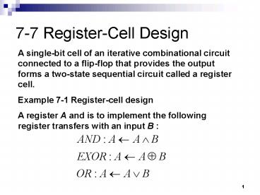
7-7 Register-Cell Design
A single-bit cell of an iterative combinational
circuit connected to a flip-flop that provides
the output forms a two-state sequential circuit
called a register cell. Example 7-1
Register-cell design A register A and is to
implement the following register transfers with
an input B
2
Example 7-1
- Assumption
- Only one of AND, EXOR, and OR is equal to 1
- For all AND, EXOR, and OR equal to 0, the content
of A remains unchanged
3
Example 7-1
- One solution
- LOADANDEXOROR
From Table 7-11, we can rewrite the solution as
4
Example 7-1
- Simplify the equation
- Share the control variables to all register cells
since they are the same for each cell - Simplification from 2nd solution in the previous
slide
5
Example 7-1
- Simplification from the 1st solution in slide
page 3
6
Example 7-1
- Use the simplification in slide page 4 can save
about 40 (for 16 cells) gate cost and hence time
delay compared to those by using the
simplification in slide page 5. - Why?
7
Example 7-2
A register A is to implement the following
register transfers with an input B
- Assumption
- Only one of SHL, EXOR, and ADD is equal to 1
- For all SHL, EXOR, and ADD equal to 0, the
content of A remains unchanged
8
Example 7-2
- Solution
- LOADANDEXOROR
- Another solution (combine ADD and SHL (share Ci))
9
Example 7-2
- Simplification (from 2nd solution in previous
slide) (Ci0 for EXOR)
10
11
7-8 Multiplexer and bus-based transfers for
multiple register
- Dedicated multiplexer
- 2n AND gate cost and n OR gate cost per
multiplexer - Total of 9n gate cost
12
Single bus
- 3n AND gate cost and n OR gate cost
- Total of 4n gate cost
13
Single bus
Note The 3rd case in the table is possible for
dedicated multiplexer architecture
14
Three-state bus
15
7-9 Serial transfer and Microoperations
- Information in a system is transferred or
manipulated one bit at a time
16
Serial transfer
17
Serial Addition
18
We are now neglecting the following two
sections7-10 Two design examples7-11 HDL
19
7-13 Microprogrammed Control
- A control unit with its binary control values
stored as words in memory - Each word in the control memory contains a
microinstruction - A microinstruction specifies one or more
microoperations for a system - A sequence of microinstructions constitutes a
microprogram
20
Two registers
- Control address register (CAR) a register
specifies the address of the microinstruction - Control data register (CDR) a register holds the
microinstruction currently being executed by the
datapath and the control unit
21
Next-address generator
- When a microinstruction is executed, the
next-address generator produces the next address - The address of next instruction to be executed
may be next one or located somewhere else in the
control memory - A function of control word is to determine the
address of the next microinstruction to be
executed - Sometimes it is called sequencer
22
Microprogrammed control unit organization
23
CISC
- A simple instruction set computer (SISC) as
introduced above cant fit the complex
applications for todays computer. - A complex instruction set computer (CISC) has
emerged (Chap. 11)
Recommended
CrystalGraphics Presentations


