
Future Technology Dec. 1, 1998 - PowerPoint PPT Presentation
Title:
Future Technology Dec. 1, 1998
Description:
Flash memory Programmable logic Distant future Atomic scale storage ... – PowerPoint PPT presentation
Number of Views:146
Avg rating:3.0/5.0
Title: Future Technology Dec. 1, 1998
1
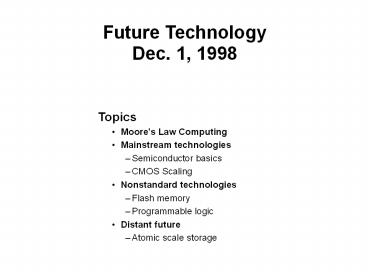
Future TechnologyDec. 1, 1998
- Topics
- Moores Law Computing
- Mainstream technologies
- Semiconductor basics
- CMOS Scaling
- Nonstandard technologies
- Flash memory
- Programmable logic
- Distant future
- Atomic scale storage
2
Impact of Technology
- Its the Technology, Stupid!
- Computer science has ridden the wave
- Things Arent Over Yet
- Technology will continue to progress along
current growth curves - For at least 10 more years
- Difficult technical challenges in doing so
- Even Technologists Cant Beat Laws of Physics
- Quantum effects create fundamental limits as
approach atomic scale - Opportunities for new devices
3
Risk of Predicting the Future
- Incremental Improvements Exceed Wildest Dreams
- Silicon CMOS
- Magnetic disks
- DRAM
- Hopes for Future Technology Never Materialize
- Magnetic bubble memory
- CCD memory
- Gallium Arsenide
- Observations
- In this business, incrementing is by
multiplicative factor - Economies of scale favor existing technology
- Shifts occur due to new market forces
- Drive for low power due to desire for portability
- Emphasis on networking due to WWW
4
Impact of Moores Law
- Moores Law
- Performance factors of systems built with
integrated circuit technology follow exponential
curve - E.g., computer speed / memory capacities double
every 1.5 years - Implications
- Computers 10 years from now will run 102 X faster
- Problems that appear intractable today will be
straightforward - Must not limit future planning with todays
technology - Example Application Domains
- Speech recognition
- Will be routinely done with handheld devices
- Breaking secret codes
- Need to use large enough keys
5
Solving Exponentially Hard Problems
- Conventional Wisdom
- Exponential problems are intractable
- Operation
- Assume problem of size n requires 2n steps
- Each step takes k years on a Y2K computer
- Y2K Computer Performance
- Start computation Jan. 1, 2000
- Keep running same machine until problem solved
- Would take k 2n years
6
Solving with a Y2K Computer
7
Moores Law Computer
- Operation
- Start computing on Jan. 1, 2000
- Keep upgrading machine being used
- In year y, would have performance 1.587y relative
to Y2K machine - Performance
- After y years of operation, would have performed
as much computation as Y2K machine would do in
time - Examples
- y 1 1.27
- y 2 3.29
- y 5 20.
- y 10 218
- y 100 2.53 X 10²⁰
8
Solving Hard Problems
- Solution Time
- Problem of size n
- Running y years on Moores Law computer
- For large values of n
- Complexity
- Linear in problem size
9
Solving with a Moores Law Computer
10
Effect of Step Complexity
- Observe
- Step complexity k adds only additive factor of
2.16 ln k to running time - Example
- For n 100
- k y
- 1 second 111
- 1 minute 120
- 1 hour 129
- 1 day 136
- 1 week 140
- 1 year 148
- Explanation
- Final years of computation will be on
exponentially faster machines
11
Implications of Moores Law
- PNP (Effectively)
- Problems of exponential complexity can be solved
in linear time - Caveat
- Cannot hold forever
- Fundamental Limit
- Argument due to Ed Fredkin
- Claim that ulimate limit to growth in memory
capacity is cubic - Cannot build storage device with less than one
electron - Assume consume all available material to build
memories - Would soon exhaust planetary resources
- Cannot travel into outer space faster than speed
of light - Total amount of material available at time t is
?(t3) - This limit will be hit in 400 years
12
Dimensions
1997 devices (0.25 µm)
Chip size (1 cm)
Diameter of Human Hair (25 µm)
1996 devices (0.35 µm)
2007 devices (0.1 µm)
Silicon atom radius (1.17 Å)
Deep UV Wavelength (0.248 µm)
X-ray Wavelength (0.6 nm)
13
MOS Transistor
Polysilicon Gate
SiO2 Gate Oxide
n
n
tox
p
Source
Drain
Silicon Substrate
- Typical Dimensions
- 1997 l 0.20 µm tox 4.5 nm
- 2007 l 0.08 µm tox ??
14
Transistor Operation
- Off
0.0 V
0.0 V
1.8 V
Excess of Free Electrons Deficit of Free
Electrons
Reverse-biased junction
On
50 100 µA
15
Scaling to 0.1µm
- Semiconductor Industry Association, 1992
Technology Workshop
Year 1992 1995 1998 2001 2004 2007 Feature
size 0.5 0.35 0.25 0.18 0.12 0.10 DRAM
cap 16M 64M 256M 1G 4G 16G Gates/chip 300K 800K 2M
5M 10M 20M Chip cm2 2.5 4.0 6.0 8.0 10.0 12.5 Int
ercn. levels 3 45 5 56 6 67 Supply
Volts 5.0 3.3 2.2 2.2 1.5 1.5 I/Os 500 750 1500 20
00 3500 5000 off chip MHz 60 100 175 250 350 500 o
n chip MHz 120 200 350 500 700 1000
16
Where are We on Roadmap?
- Semiconductor Industry Association, 1992
Technology Workshop - Compare to 1998 state of the art (Pentium II Xeon)
Year 1998 Xeon Status Feature size 0.25 0.25 On
track DRAM cap 256M Available Gates/chip 2M 7.5M
xtrs What did they mean? Chip cm2 6.0 1.18 Nobody
gt 4.75 Intercn. levels 5 4 (Others) On
target Supply Volts 2.2 2.0 Early I/Os 1500 528 No
body gt 1088 off chip MHz 175 100 Others
faster on chip MHz 350 450 Early
17
Challenges Reaching 0.1 µm
- Gate oxide tunneling
- electrons jump through thin gate oxides
- Nonuniform dopant concentrations
- lt 100 dopant atoms in inversion layer
- Statistical variations cause varying device
characteristics - Scaling of threshold voltages
- Difference between gate and source voltages for
transistor to turn on - Too low leakage current when transistor off
- Higher standby power
- Too high poor performance
- Lithography
- Reaching optical limits
- Alternatives (X-ray, E-beam) costly for large
scale manufacturing
18
Sub 0.1 µm Devices
- Double Gate MOS Transistor
- IBM J. RD, Jan/Mar 95
- Thin channel region allows more effective shutoff
- How low can you go?
- Below 10nm (0.01 µm), quantum effects become
prevalent - This would be 1000 X improvement over todays
areal densities
19
Scaling Theory
- Constant Field Scaling
- Rideout, et al, IBM 77
- Uniformly scale all linear dimensions by factor
of ? - Also reduce supply voltage by factor of ?
- Preserves field strength
- E V/d
- Otherwise get breakdown effects
- In reality, not scaling as quickly as linear
dimensions
1/?
20
Effect of Scaling
- Transistor Count
- Assuming constant area ? ?2
- Actual chips are growing slowly
- Switching Time
- Channel Length / Field ? 1/?
- Capacitances
- Area / Distance ? 1/?
- Switching Power / Device
- Frequency 1/switching time ? ?
- C V2 Frequency ? 1/?2
- Power / Chip
- Device Power devices ? 1
- In reality, growing to allow increased
performance
21
Scaling the Wires
W
L
H
T
- Scaled Wires
- All dimensions shrink by ?
- Resistance R
- L/(HW) ? ?
- Capacitance to Substrate C
- LW/T ? 1/?
- Wire Delay
- RC ? 1
- Relative to switching ? ?
- Becomes dominating factor
22
Scaling the Wires (cont)
W
L
H
T
- Cross-Chip Wires
- Only height H and width W shrink by ?
- Resistance R
- L/(HW) ? ?2
- Capacitance to Substrate C
- LW/T ? 1
- Wire Delay
- RC ? ?2
- Relative to switching ? ?3
- Appears to be impractical
23
Adding Repeaters
- Repeaters
- Act as amplifiers
- Implemented using inverters
- Assume Insert k Repeaters
- Each has delay ? (R/k C/k) ? RC/k2
- Total delay k(? RC/k2) k? RC/k
- Minimum delay 2SQRT(RC?)
- Scales as SQRT(?)
24
Real-Life Scaling
- Dont drop supply voltage as fast
- Higher speed at cost of higher power
- Dont shrink wires uniformly
- Increase Vertical/Horizontal aspect ratio
- Problem Parasitic Capacitances to adjacent wires
dominate - Major problem for CAD tools
25
Processing Tricks
- Low Resistivity Interconnect
- Use copper rather than aluminum
- Provides 1.8X improvement
- Low Dielectric Constant Insulators
- Especially for space between adjacent wires
- Reduces parasitic capacitances
- Provides 2X improvement
26
Wire Scaling
- Mark Bohr, Intel, IEDM 95
- Wire
- 43um long
- 0.8um high
- Scaled width
27
Nonstandard Technology
- Flash Memory
- Provides nonvolatile storage
- Maintains state when power turned off
- Features slow write, but reasonable read
- RAM Programmable Logic
- Hardware that can be dynamically reconfigured
- Both functionality and wiring connections
programmable - Blurs distinction between hardware and software
- Microdisk Storage Arrays
- Future technology for large scale storage systems
28
Flash Memory
- Characteristics
- Retains state even when power shut off
- Read times comparable to DRAM
- Slow write times
- Limited endurance 100,000 read/write cycles
(or less!) - Applications
- Semi-permanent storage
- Built in software, parameter RAM, font tables
- Endurance and slow writes not an issue
- Alternative to magnetic storage
- No moving partslower power and more rugged
- More expensive per bit Approx. 2X DRAM
29
Flash Memory Cell
- Samsung, IEDM 95
- Cell Size 1.6 µm2
- 1.4 X denser than DRAM cell for comparable design
rules - Simpler process
- Cross Section
- Two Cells
- Common control gate
- Common source
30
Flash Cell Writing
- Based on Fowler-Nordheim Tunneling
- Electron has nonzero probability of crossing thin
insulator - Erase Operation
- Drive electrons into floating gate
- For entire group of cells
- Program Operation
- Drive electrons out of floating gate
- For selected cell
- State Retention
- Electrons will remain in floating gate
indefinitely
31
How Tunneling Works
Window
Wind
Average Energy Level
- Average electron energy insufficient to mobilize
- Statistical variation in energies
- Especially energetic ones can mobilize
32
Erasing Flash Cells
- Erasing
- Electrons drawn into floating gate
- For entire group of cells
- 400 µs
33
Programming Flash Cell
- Electrons pushed out of floating gate
- For selected cell
- 15 µs
Programming Upper Right Cell
0v (Column Deselect)
5v (Column Select)
Selected
v (Activate Drains)
-11v (Row Select)
0v (Row Deselect)
11v
Deselected
0v (Row Deselect)
float
0v
0v (Float Source)
34
Flash Cell Reading
Programmed Cell
Erased Cell
5v
5v
0v
1v
0v
1v
- Behaves like normal transistor
- But, lower quality
- Threshold voltage 2 v
- Trapped electrons shield control gate
- Treshold voltage 7 v
35
Reliability
- State Retention
- Electrons stay trapped in floating gate
- Good for 10 years
- Endurance
- Over many erase / program cycles, electrons
become trapped in tunneling oxide - OK for 100,000 cycles
- Causes threshold voltage for programmed cell to
rise
36
Intel StrataFlash
- Microprocessor Report 10/6/97, Intel WWW site
- Process Technology
- 0.4µm process
- 50,000 electrons in single cell
- Multi-Valued Storage
- 4 different programming levels / cell
- 5 added to die area for enhanced read/write
circuitry - 150 ns read access time
- 32-byte write buffer with 6 µs / byte write time
- Erase in 128 KB blocks
- Up to 10,000 erase cycles / block
- Takes 1s
- Availability
- 64Mb chip
- 30 list for quantities gt 10,000
37
Field Programmable Gate Arrays
- Chip Populated with Programmable Elements
- Programmable Logic Blocks
- Programmable Routing Resources
- Configuration Determines Functionality
- On-chip SRAM cells hold programming bits
- Configured as shift register for downloading
- Effect
- Speed comparable to conventional hardware
(multi-megahertz) - Flexibility ability to change comparable to
software
38
Programmable Logic Cells
- Lookup Table (LUT) based
- Store the truth table of n-input logic function
- Requires 2n bits of configuration
- Xilinx 4000 parts 4-input LUTs
2-input LUT
AB 00 01 10 11
0 0 0 1
39
60 bits of configuration information
LUT
LUT
LUT
Programmable Cell for Xilinx XC4000 Single chip
contains 56 X 56 cell array
40
Xilinx Interconnect
- Programmable Interconnect
- Pass Transistors as switches
Usable by another net.
0
1
Stored bits determine switch state.
0
1
41
Routingfor SingleCell
- Different length wires
- Varying performance
- Special carry logic
42
Applications of FPGAs
- Currently
- Hardware prototyping emulation
- Systems where anticipate need to change
functionality - E.g., protocols yet to be standardized
- Potentially
- Programmable logic mixed with hard-wired in CPU
core - Reconfigure for specialized functions,
nonstandard data types, etc. - Instruction set extensions in style of MMX, but
more flexible - Research projects at CMU
- Seth Goldstein, Herman Schmit
- Course offered next semester
43
Micro Disks
- Motivation
- Current disk drives give high capacity but poor
access times - Mechanical components limit reliability and
consume power - Microelectronic Mechanical Systems (MEMS)
- Fabricate mechanical devices using VLSI
processing technology - Currently used for miniaturized sensors and
actuators - Silicon Disk
- Proposed technology for high density storage
- Goal is to get 100 Gb in 1cm2
- 3 nm X 3 nm bit storage
- 1 of surface used for bit storage
- Rest for electronics and actuators
44
Storage Array
- Probe tip moves over 32 X 32 array of bits
- Arm controlled by electrostatic actuator
- Uses tunneling to read/write bits
Recommended
CrystalGraphics Presentations


