
Sn - PowerPoint PPT Presentation
Title:
Sn
Description:
Effect of sputter-particle flux variations on properties of ZnO:Al thin films ... Static diode mode of sputtering Dynamic magnetron mode of sputtering Introduction – PowerPoint PPT presentation
Number of Views:43
Avg rating:3.0/5.0
Title: Sn
1
Effect of sputter-particle flux variations on
properties of ZnOAl thin films
S. Flickyngerova1, M. Netrvalova2,L. Prusakova2,
I. Novotny1, P.Sutta2 , V. Tvarožek1, A.
Pullmannova1
1Department of Microelectronics, Slovak
University of Technology, Ilkovicova 3, 812 19
Bratislava, Slovakia 2Department New
Technologies Research Center, The University of
West Bohemia, Univerzitni 8, 306 14 Plzen, Czech
Republic
Static diode mode of sputtering
Dynamic magnetron mode of sputtering
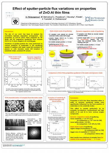
Introduction The aim of our work has been to
analyze the correlation between deposition
arrangement and properties of ZnOAl (AZO) films
prepared by RF diode and RF magnetron sputtering
from ceramic ZnO2 wt. Al2O3 targets in Ar
working gas. Variations of sputter-particle flux
were performed by various positions of substrates
in the sputtering system in addition with static
mode SM (constant RF power) or with dynamic mode
DM (rotation of substrate holder, constant RF
power).
- 5 samples were fitted on circular rotated
substrate holder - ceramic target AZO ( 76 mm in diameter) is
eccentrically placed 150 mm under the substrate
holder which is rotating at 96 rpm - for middle sample position x 0 mm
- sputtering power 400 W, at room temperature
for 90 min
- 14 samples were placed on circular substrate
holder under AZO target - ceramic target, ZnO2 wt. Al2O3, with
diameter of 152 mm - for middle sample position x 0 mm
- sputtering power 800 W, at room temperature
for 17 min
Static diode mode of sputtering
Dynamic magnetron mode of sputtering
Comparison of thin films properties sputtered in
the static and dynamic mode
Evolution of the electrical resistivity, biaxial
lattice stress and crystallite size vs. sample
position of AZO films deposited in the diode
static mode and magnetron dynamic mode
Plot of normalized electrical resistivity,
integral transmittance and the optical band gap
as a function of the sample position on the
substrate holder
Evolution of resistivity optical band gap with
biaxial stress
TEM characterization of samples from the static
mode
Conclusion Properties of AZO thin films deposited
either in static or dynamic sputtering modes were
significantly influenced by the local position of
substrates on the substrate holder. This effect
is caused particularly by an energetic
ion-/electron- bombardment and high ability of Zn
and Al to form various oxygen compounds.
(a)
(b)
Plan view TEM micrograph of ZnOAl thin films.
The mean grain size is approx. 50 nm for middle
sample (a) 20 nm for peripheral sample (b)
Dynamic magnetron mode of sputtering lower
resistivity ? 4.6 10-3 ?cm (in
comparison 4.1 10-2 ?cm for SM)lower lattice
stress - 2.8 GPa (in comparison
- 6.41 GPa for SM)
Normalized electrical resistivity as a function
of the biaxial lattice stress for static and
dynamic sputtering mode
Cross-sectional TEM micrograph (bright field
image) of ZnOAl thin film reveals the columnar
structure
Static diode mode of sputteringhigher integral
transmittance T 91
(in comparison 86 for DM)bigger size of
crystalitte D 134 nm
(in comparison 108 for DM)
Electron diffraction confirms the hexagonal
ZnOAl phase reveals the preferential orientation
(001) in normal to the film plane direction. ED
is taken at beam perpendicular to the film plane
Optical band gap as a function of the biaxial
lattice stress for static and dynamic sputtering
mode
Best results were obtained at samples from the
middle of the substrate holder ? x 0 mm
Corresponding author sona.flickyngerova_at_stuba.sk
Special thanks to Dr. I. Vavra for TEM analyses
Recommended
CrystalGraphics Presentations


