
The Scale Vector-Thread Processor - PowerPoint PPT Presentation
Title:
The Scale Vector-Thread Processor
Description:
The Scale Vector-Thread Processor Computer Science and Artificial Intelligence Laboratory slt slt psel psel slt sll psel lw Ronny Krashinsky, Christopher Batten ... – PowerPoint PPT presentation
Number of Views:26
Avg rating:3.0/5.0
Title: The Scale Vector-Thread Processor
1
The Scale Vector-Thread Processor
Computer Science and Artificial
Intelligence Laboratory
Ronny Krashinsky, Christopher Batten, Krste
Asanovic http//cag.csail.mit.edu/scale
Vector-Thread Architecture
Scale Prototype Chip in TSMC 0.18µm
Standard Cell Preplacement
Chip Statistics
Initial Results
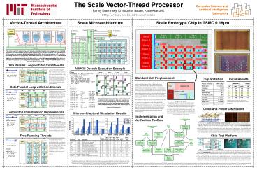
We have developed a C based preplacement
framework which manipulates standard cells using
the OpenAccess libraries. Preplacement has
several important advantages including improved
area utilization, decreased congestion, improved
timing, and decreased tool run time. The
framework allows us to write code to instantiate
and place standard cells in a virtual grid and
programmatically create logical nets to connect
them together. The framework processes the
virtual grid to determine the absolute position
of each cell within the preplaced block. We
preplaced 230 thousand cells (58 of all standard
cells) in various datapaths, memory arrays, and
crossbar buffers and tri-states. After
preplacing a block, we export a Verilog netlist
and DEF file for use by the rest of the toolflow.
Although the preplaced blocks do not need to be
synthesized, we still input them into the
synthesis tool so that the tool can correctly
optimize logic which interfaces with the
preplaced blocks. During place route we use
TCL scripts to flexibly position the blocks
around the chip. Although we preplace the
standard cells, we do the datapath routing
automatically we have found that automatic
routing produces reasonably regular routes for
signals within the preplaced blocks.
Process Technology TSMC 0.18µm
Metal Layers 6 aluminum
Transistors 7.14 M
Gates 1.41 M
Standard Cells 397 K
Flip-Flops Latches 94 K
Core Area 16.61 mm2
Chip Area 23.14 mm2
Design Time 19 months
Design Effort 24 person-months
Voltage (V) Maximum Frequency (MHz) Power (mW) Energy per Cycle (nJ)
1.2 157 156 0.99
1.5 218 342 1.57
1.8 270 612 2.27
2.1 304 955 3.14
2.4 338 1404 4.15
Initial results for running the adpcm.dec
benchmark from on-chip RAM with no cache tag
checks
Clock and Power Distribution
Microarchitectural Simulation Results
1 Lane
2 Lanes
4 Lanes
The chip includes a custom designed
voltage-controlled oscillator to enable testing
at various frequencies. Scale can either be
clocked by the on-chip VCO or by an external
clock input. The clock tree was automatically
synthesized using Encounter and the maximum
trigger-edge skew is 233ps. Scale uses a
fine-grained power distribution grid over the
entire chip as show in the above diagrams. The
standard cells have a height of nine Metal 3/5
tracks and the cells get power/ground from Metal
1 strips which cover two tracks. We horizontally
route power/ground strips on Metal 5, directly
over the Metal 1 power/ground strips, leaving
seven Metal 3/5 tracks unobstructed for signal
routing. We vertically route power/ground strips
on Metal 6. These cover three Metal 2/4 tracks
and are spaced nine tracks apart. The power
distribution uses 21 of the Metal 6 and 17 of
Metal 5.
8 Lanes
Kernel Speedup
Chip Test Platform
Benchmark Suite Description Kernel Speedup Ops Per Cycle Ld-El Per Cycle St-El Per Cycle Mem-B Per Cycle Loop Types Memory Access Types
rgbcmyk EEMBC RGB to CMYK color conversion 14.8 6.8 1.2 0.4 3.0 DP VM,SVM
rgbyiq EEMBC RGB to YIQ color conversion 39.8 9.3 1.3 1.3 3.8 DP SVM
hpg EEMBC High pass gray-scale filter 44.6 10.4 2.8 1.0 3.1 DP VM,VP
fft EEMBC 256-pt fixed-point complex FFT 18.8 3.8 1.7 1.4 0.1 DP VM,SVM
viterbi EEMBC Soft decision Viterbi decoder 10.5 5.0 0.5 0.5 0.1 DP VM,SVM
dither EEMBC Floyd-Steinberg gray-scale dithering 6.9 5.0 1.1 0.3 0.3 DP,DC VM,SVM,VP
lookup EEMBC IP route lookup using Patricia Trie 5.8 6.9 0.9 0.0 0.0 DC VM,VP
pktflow EEMBC IP packet processing (2MB dataset) 13.5 3.7 0.7 0.1 4.2 DC,XI VM,VP
sha MiBench Secure hash algorithm (large dataset) 2.4 1.9 0.3 0.1 0.0 DP,XI VM,VP
adpcm.enc MediaBench Speech encoding 1.9 2.3 0.1 0.0 0.0 XI VM,VP
adpcm.dec MediaBench Speech decoding 8.1 6.7 0.6 0.2 0.0 XI VM,VP
ptrchase EEMBC Pointer chasing, searching linked lists 4.4 2.3 0.3 0.0 0.0 FT VP
quicksort MiBench Quick sort of short strings (small dataset) 3.0 2.0 0.4 0.3 2.2 FT VP
The chip test infrastructure includes a host
computer, a test baseboard, and a daughter card
with a socket for Scale. The test baseboard
includes a host interface and a memory controller
implemented on a Xilinx FPGA as well as 96MB of
SDRAM, configurable power supplies, and a tunable
clock generator. The host interface is clocked
by the host and uses a low-bandwidth asynchronous
protocol to communicate with Scale, while the
memory controller and the SDRAM use a synchronous
clock generated by Scale. Using this test setup,
the host computer is able to download and run
programs on Scale while monitoring the power
consumption at various voltages and frequencies.
To allow us to run real programs which include
file I/O and other system calls, a simple proxy
kernel marshals up system calls, sends them to
the host, and waits for the results before
resuming program execution.
Kernel speedup is compared to compiling the
benchmark and running it on the Scale control
processor. Mem-B is average number of bytes of L1
to main memory traffic per cycle. Ld-El and St-El
are number of load and store elements transferred
to and from the cache per cycle. Loop types
include data parallel loops with no control flow
(DP), data parallel loops with control flow or
inner loops (DC), loops with cross-iteration
dependencies (XI), and free running threads (FT).
Memory access types include unit-stride and
strided vector memory accesses (VM), segment
vector memory accesses (SVM), and individual VP
loads and stores (VP).
This work was partially supported by a DARPA
PAC/C award, an NSF CAREER award, an NSF graduate
fellowship, a CMI research grant and donations
from Infineon Technologies and Intel. We
acknowledge and thank Albert Ma for designing the
VCO and providing extensive help with CAD tools,
Mark Hampton for implementing VTorture and the
Scale compilation tools, Jaime Quinonez for the
baseline datapath tiler implementation, Jared
Casper for work on an initial cache design and
documentation, and Jeffrey Cohen for initial work
on VTorture.
Recommended
CrystalGraphics Presentations


